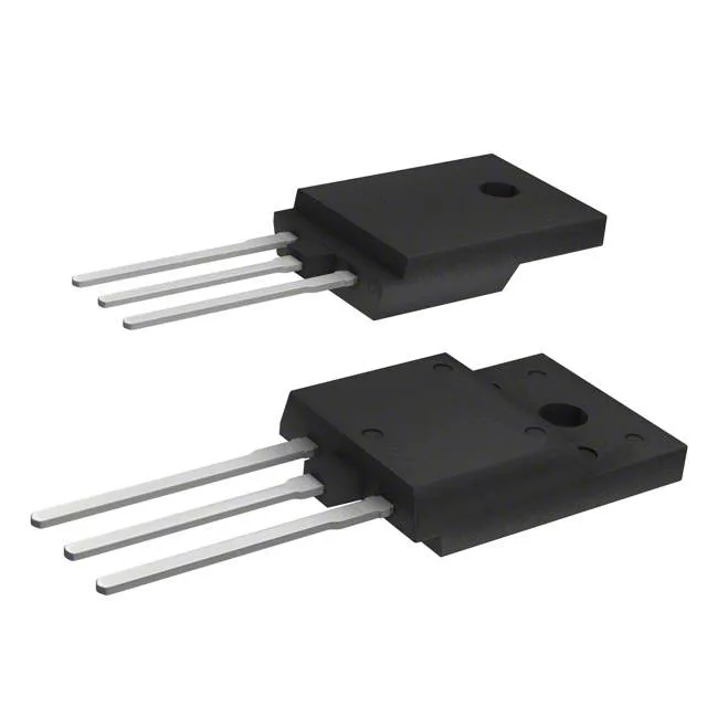
STMicroelectronics STFW4N150 — Discrete Semiconductors

STMicroelectronics STFW4N150 N-Channel MOSFET, 1500 V, 4 A

MPNSTFW4N150
Active

STMicroelectronics PowerMESH™ N-Channel MOSFET, STFW4N150, 1500 Vdss, 4 A Id, 7 Ohm Rds(on) at 10 V, TO-3P-3 Full Pack (TO-3PF), Through Hole, 63 W power dissipation.

$6.1000Ref. price · indicative, final on quote
Sourced new & surplus through independent channelsAuthenticity-screened · ESD-safe packingListing updated Aug 2026

Specifications

STFW4N150 specifications
ParameterValue
SeriesPowerMESH™
FET typeN-Channel
MountingThrough Hole
Drain to source voltage1500 V
Drive voltage (Max rds on, min rds on)10V
Current - continuous drain (Id) @ 25°C4A (Tc)
Power dissipation63W (Tc)
Operating temperature150°C (TJ)
PackageTube
Vgs±30V
TechnologyMOSFET (Metal Oxide)
CaseTO-3P-3 Full Pack
Vgs(th) (Max) @ id5V @ 250µA
Rds on (Max) @ id, vgs7Ohm @ 2A, 10V
Gate charge (Qg) (Max) @ vgs50 nC @ 10 V
Input capacitance (Ciss) (Max) @ vds1300 pF @ 25 V

Product details

1500 V N-channel in a full-pack isolated tab

The STMicroelectronics STFW4N150 is a 1500 V, 4 A N-channel PowerMESH MOSFET in a TO-3PF full-pack through-hole package. The 1500 V drain-source rating places it squarely in high-voltage offline applications — flyback converters, PFC stages, two-switch forward converters, and auxiliary power supplies where the primary-side rail runs off rectified mains.

7 Ohm Rds(on) — conduction loss budget

On-resistance is specified at 7 Ohm maximum with 10 V gate drive at 2 A drain current. That is a relatively high figure compared to low-voltage switching FETs, but at 1500 V the die is sized for voltage blocking, not low Rds(on). Conduction loss at 2 A is I²R = 28 W, which consumes nearly half the 63 W power dissipation budget at 25°C case temperature. Practical designs will run at lower duty cycles or lower average currents to stay inside the SOA.

That is modest — a standard gate driver IC or a simple resistor-capacitor drive network can charge the gate in a few hundred nanoseconds. The 50 nC Qg means the gate drive power at 100 kHz switching is Pgate = Qg × Vgs × fsw = 50 nC × 10 V × 100 kHz = 50 mW, easily handled by a small driver. The 1300 pF Ciss keeps the Miller plateau short, so switching losses in a resonant or quasi-resonant topology stay manageable.

The base product number is STFW4, which covers the family variants — confirm the exact suffix for your BOM line.

Frequently asked questions

What is the Vgs threshold of STFW4N150?

The maximum gate-source threshold voltage is 5 V at 250 µA drain current. The recommended drive voltage for minimum on-resistance is 10 V.

What is the closest pin-compatible alternative to STFW4N150?

STMicroelectronics offers the STFW4N150 in the PowerMESH family with the TO-3PF package. Pin-compatible alternatives within the same voltage class would be other TO-3PF N-channel MOSFETs from the STW series — verify the footprint and gate drive requirements against your specific design before substituting.