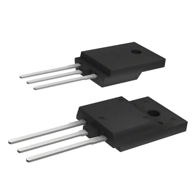
STMicroelectronics STFW45N65M5 — Discrete Semiconductors

STFW45N65M5 N-Channel MOSFET, 650 V, 35 A, MDmesh V, TO-3PF

MPNSTFW45N65M5
Active

STMicroelectronics MDmesh™ V, N-Channel MOSFET, 650 V Vdss, 35 A Id, 78 mOhm Rds(on) @ 10 V, 82 nC Qg, TO-3PF-3 Full Pack, Through Hole, 150°C Tj.

$6.1833Ref. price · indicative, final on quote
Sourced new & surplus through independent channelsAuthenticity-screened · ESD-safe packingListing updated Aug 2026

Specifications

STFW45N65M5 specifications
ParameterValue
SeriesMDmesh™ V
FET typeN-Channel
MountingThrough Hole
Drain to source voltage650 V
Drive voltage (Max rds on, min rds on)10V
Current - continuous drain (Id) @ 25°C35A (Tc)
Power dissipation57W (Tc)
Operating temperature150°C (TJ)
PackageTube
Vgs±25V
TechnologyMOSFET (Metal Oxide)
CaseTO-3P-3 Full Pack
Vgs(th) (Max) @ id5V @ 250µA
Rds on (Max) @ id, vgs78mOhm @ 17.5A, 10V
Gate charge (Qg) (Max) @ vgs82 nC @ 10 V
Input capacitance (Ciss) (Max) @ vds3470 pF @ 100 V

Product details

650 V N-channel MDmesh V MOSFET in TO-3PF full-pack

The STMicroelectronics STFW45N65M5 is an N-channel power MOSFET built on the MDmesh™ V technology, designed for high-voltage switching applications.

Conduction and switching losses — the numbers that matter

The on-resistance is specified at 78 mOhm maximum when driven with 10 V gate voltage at 17.5 A drain current. That 78 mOhm figure is at 25°C junction temperature; at 125°C junction it roughly doubles, so budget conduction loss accordingly for continuous operation. The gate charge totals 82 nC at 10 V, which sets the drive energy per switching cycle and the average gate-drive current needed at the target frequency. Input capacitance measures 3470 pF at 100 V drain-source, a figure that feeds into the switching-time estimate and the driver's peak current requirement.

Thermal and operating limits

Maximum junction temperature is 150°C, and the device is rated for a power dissipation of 57 W at case temperature. The TO-3PF package has a lower thermal mass than a standard TO-247, so the dissipation limit is package-constrained; plan the heatsink and airflow to keep junction temperature under 125°C for reliable long-term operation. The operating temperature limit covers the junction only — storage temperature is not separately stated, but standard handling precautions apply.

For production BOMs, the active status removes last-time-buy risk for new designs.

Frequently asked questions

What are the thermal limits for STFW45N65M5 in a TO-3P package?

The maximum junction temperature is 150°C, and the device is rated for 57 W power dissipation at case temperature. The TO-3PF full-pack package provides an isolated tab, simplifying heatsink mounting, but its thermal resistance is higher than a standard TO-247 — plan the thermal solution accordingly.

Can STFW45N65M5 be used in a power supply design?

Yes, the 650 V drain-source rating and 35 A continuous current capability make it suitable for power-factor-correction stages, flyback converters, and resonant-switching power supplies. The 82 nC gate charge and 78 mOhm on-resistance support efficient switching at moderate frequencies.

Is STFW45N65M5 a direct replacement for STFW45N65M4?

The STFW45N65M5 is from the MDmesh V series, while the STFW45N65M4 belongs to the earlier MDmesh IV generation. Both are 650 V, 35 A N-channel MOSFETs in the same TO-3PF package, but the MDmesh V typically offers lower Rds(on) and improved switching figures of merit. Check the specific Rds(on) and gate charge values for your operating point before substituting — the pinout is the same, but the gate-drive and loss budget may differ.