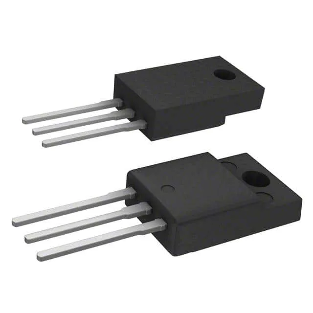
ST lists the STFV4N150 as Obsolete.
Gate charge and input capacitance — drive and switching budget
These numbers size the gate-drive circuit: a 10 V drive voltage is required to achieve the rated on-resistance. The 50 nC Qg means a typical gate driver with 1 A peak source/sink can switch the device in the tens of nanoseconds range, but the isolated TO-220 package adds lead inductance that slows the edge — account for it in the gate-loop layout. The 1300 pF Ciss at 25 V Vds is moderate for a 1500 V device; it does not demand an unusually strong driver, but the Miller plateau will be visible on the gate waveform.
Thermal and power handling in the Full Pack
Maximum power dissipation is 40 W at case temperature, and the junction temperature rating is 150 °C. The TO-220 Full Pack has higher thermal resistance than a standard TO-220 because the plastic encapsulation surrounds the die — the junction-to-case thermal path is through the mould compound, not a metal tab. In practice, the 40 W ceiling is reachable only with a large heatsink and good thermal interface. For continuous operation at 4 A, the 7 Ohm Rds(on) produces 112 W conduction loss at full current — clearly the 4 A rating is a pulsed or short-duration maximum, not a steady-state figure at 1500 V. Derate aggressively for linear-mode or switching applications with high duty cycles.