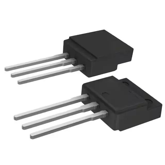
STMicroelectronics STFI6N62K3 — Discrete Semiconductors

STFI6N62K3 N-Channel MOSFET, 620 V, 5.5 A, SuperMESH3™

MPNSTFI6N62K3
Obsolete

STMicroelectronics SuperMESH3™ N-Channel MOSFET, 620 V Vdss, 5.5 A Id, 1.2 Ohm Rds(on) @ 2.8 A, 10 V, 34 nC Qg, TO-262-3 I2PAKFP through-hole.

$1.9200Ref. price · indicative, final on quote
Sourced new & surplus through independent channelsAuthenticity-screened · ESD-safe packingListing updated Jul 2026

Specifications

STFI6N62K3 specifications
ParameterValue
SeriesSuperMESH3™
FET typeN-Channel
MountingThrough Hole
Drain to source voltage620 V
Drive voltage (Max rds on, min rds on)10V
Current - continuous drain (Id) @ 25°C5.5A (Tc)
Power dissipation30W (Tc)
Operating temperature150°C(TJ)
PackageTube
Vgs±30V
TechnologyMOSFET (Metal Oxide)
CaseTO-262-3 Full Pack, I²Pak
Vgs(th) (Max) @ id4.5V @ 50µA
Rds on (Max) @ id, vgs1.2Ohm @ 2.8A, 10V
Gate charge (Qg) (Max) @ vgs34 nC @ 10 V
Input capacitance (Ciss) (Max) @ vds875 pF @ 50 V

Product details

620 V N-channel MOSFET in the I2PAKFP full-pack through-hole package

The STMicroelectronics STFI6N62K3 is a 620 V N-channel power MOSFET from the SuperMESH3™ series, built with a metal-oxide semiconductor structure. Housed in the TO-262-3 Full Pack I²Pak (I2PAKFP, TO-281) through-hole package, the fully isolated tab simplifies heatsinking without an insulating pad — the back of the package is electrically isolated, which matters when you are bolting it to a grounded chassis in an off-line power supply or lighting ballast.

1.2 Ohm Rds(on) and 34 nC gate charge — conduction and switching budget

For a 100 kHz hard-switched converter, budget the gate drive loss at roughly Qg × Vgs × fsw = 34 nC × 10 V × 100 kHz = 34 mW, which is manageable. The 4.5 V gate threshold at 50 µA means the device is fully enhanced only with a 10 V drive — do not expect clean turn-on with 5 V logic.

150°C junction temperature and through-hole mounting

The maximum operating junction temperature is 150°C, which is standard for power MOSFETs. The 30 W power dissipation at the case assumes an infinite heatsink; real designs derate based on the thermal interface. The ±30 V maximum gate-source voltage gives headroom for gate drive transients, but keep the drive voltage at 10 V for the rated Rds(on).

Frequently asked questions

Where can I buy STFI6N62K3?

The STFI6N62K3 is obsolete and no longer in factory production. Submit an RFQ to confirm current availability and pricing — stock levels and lead times are confirmed at quote time, not on the listing page.

Is STFI6N62K3 obsolete?

Yes, the STFI6N62K3 carries an Obsolete lifecycle status. Sourcing is through the surplus and broker channel.

What are the specifications of STFI6N62K3?

The STFI6N62K3 is a 620 V N-channel MOSFET from the SuperMESH3™ series. Gate charge is 34 nC at 10 V, input capacitance is 875 pF at 50 V, and the maximum junction temperature is 150°C. It comes in the TO-262-3 Full Pack I²Pak (I2PAKFP) through-hole package.