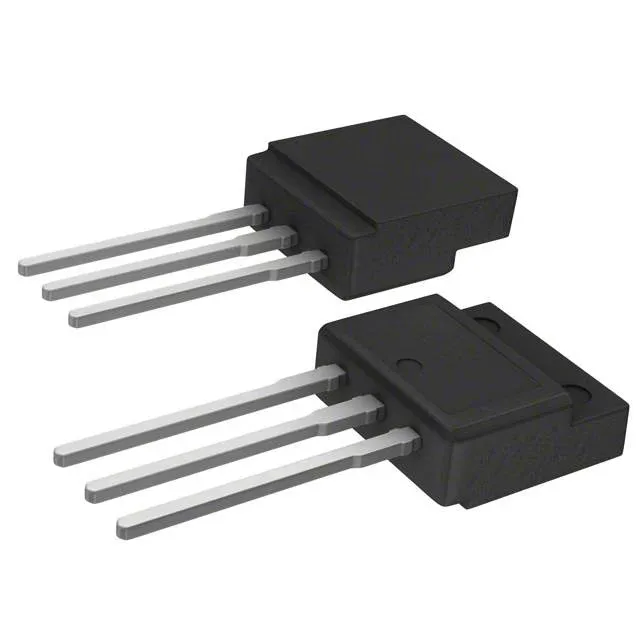
650 V superjunction MOSFET in the TO-262 Full Pack
This part is aimed at applications like AC-DC power supplies, PFC stages, and high-voltage DC-DC converters where 650 V blocking and moderate current are needed.
The 650 V Vdss gives you a solid margin for 400 V DC-link rails in power factor correction or flyback converters — typical derating practice keeps the peak drain voltage under 80% of the rating. The 190 mOhm Rds(on) at 10 V gate drive means conduction losses are manageable at 9 A, but the on-resistance roughly doubles if you try to drive the gate with 4.5 V logic — this part really wants a 10 V gate rail for lowest losses. The 45 nC gate charge is moderate; a standard gate driver with 1 A peak current will switch it in the tens of nanoseconds, but watch the gate loop inductance in the TO-262 layout to avoid ringing. The 150°C maximum junction temperature and 130 W power dissipation rating give thermal headroom, but the full-pack package has higher thermal resistance than a standard TO-220 because the plastic isolates the tab. Plan for a heatsink with good airflow if you are running near the 18 A continuous limit.