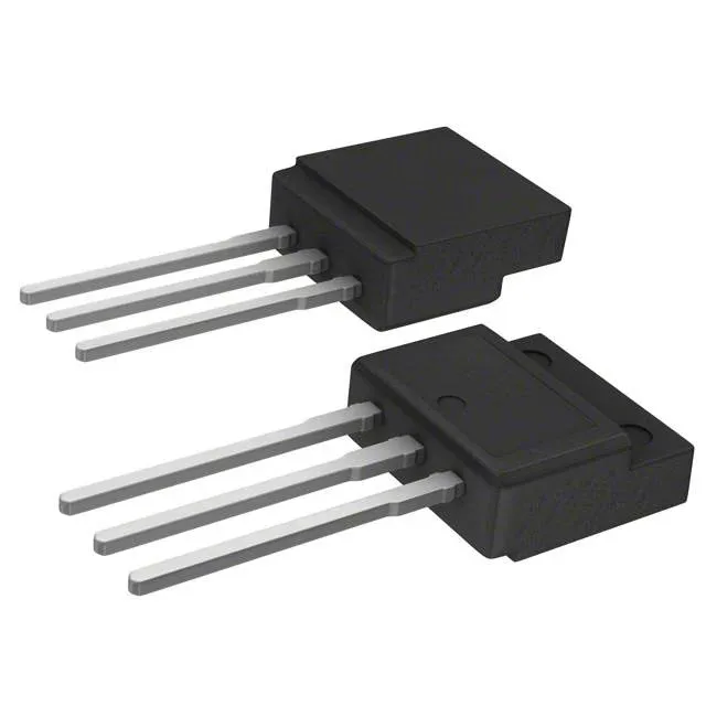
STMicroelectronics STFI15N65M5 — Discrete Semiconductors

STFI15N65M5 N-Channel MOSFET, 650 V, 11 A, 340 mOhm

MPNSTFI15N65M5
Obsolete

STMicroelectronics MDmesh™ V series, N-Channel MOSFET, 650 V drain-source, 11 A continuous drain at 25°C, 340 mOhm Rds(on) at 10 V, through-hole TO-262-3 Full Pack (I2PAKFP), 150°C junction temperature.

$2.5900Ref. price · indicative, final on quote
Independent supplier — new & surplus stockAuthenticity-screened · ESD-safe packingListing updated Jul 2026

Specifications

STFI15N65M5 specifications
ParameterValue
SeriesMDmesh™ V
FET typeN-Channel
MountingThrough Hole
Drain to source voltage650 V
Drive voltage (Max rds on, min rds on)10V
Current - continuous drain (Id) @ 25°C11A (Tc)
Power dissipation30W (Tc)
Operating temperature150°C (TJ)
PackageTube
Vgs±25V
TechnologyMOSFET (Metal Oxide)
CaseTO-262-3 Full Pack, I²Pak
Vgs(th) (Max) @ id5V @ 250µA
Rds on (Max) @ id, vgs340mOhm @ 5.5A, 10V
Gate charge (Qg) (Max) @ vgs22 nC @ 10 V
Input capacitance (Ciss) (Max) @ vds816 pF @ 100 V

Product details

For BOM lines that still require this exact order code, procurement must turn to the independent distribution channel.

The 650 V drain-source rating places it squarely in the 600 V–650 V class used for power-factor-correction stages, flyback converters, and auxiliary switched-mode power supplies in industrial and consumer equipment.

The gate is driven with 10 V for the rated Rds(on) minimum; the absolute maximum gate-source voltage is ±25 V. Total gate charge is 22 nC at 10 V, which is moderate for this voltage/current class — a typical gate driver with 1 A peak source/sink can switch the device in the 50–100 ns range, though the actual switching speed depends on the driver's output resistance and the external gate resistor. Input capacitance is 816 pF at 100 V drain-source, a value that helps keep the Miller plateau manageable for designs that need to balance switching losses against EMI.

The STFI15N65M5 comes in a TO-262-3 Full Pack (I²Pak) through-hole package, also designated I2PAKFP (TO-281). The full-pack (isolated tab) variant means the metal backside tab is electrically isolated from the drain, simplifying heatsink attachment — no insulating pad is required, though thermal grease is still recommended. The junction-to-case thermal path must handle up to 30 W power dissipation at the case temperature rating. The 150°C maximum junction temperature allows a reasonable derating window: for a 105°C ambient, the allowable temperature rise is 45°C, which at 30 W gives a required thermal resistance of 1.5°C/W or better from case to ambient — achievable with a modest heatsink and forced airflow.

Frequently asked questions

Is STFI15N65M5 obsolete?

Yes, STMicroelectronics lists the STFI15N65M5 as Obsolete. The part is available only through the independent surplus and broker channel.

What is the replacement for STFI15N65M5?

STMicroelectronics has not published an official successor order code for the STFI15N65M5 in the available records. For a drop-in replacement, a buyer should evaluate other 650 V N-channel MOSFETs in the TO-262-3 Full Pack package with similar Rds(on) and gate charge — for example, the STF15N65M5 (the TO-220FP variant) or a later-generation MDmesh part like the STF15N65M2-AG, but pin compatibility and electrical fit must be verified against the specific application's switching frequency, drive voltage, and thermal budget.

What is the Rds(on) of STFI15N65M5?

The maximum on-resistance is 340 mOhm at a gate-source voltage of 10 V and a drain current of 5.5 A.