The 650 V Vdss rating places this part in the high-voltage sweet spot for single-switch flyback converters, PFC stages, and auxiliary power supplies in industrial and telecom equipment. The 25 W power dissipation ceiling (Tc) means the junction-to-case thermal path is the limiting factor; the Full Pack package's isolated tab helps with heatsinking but adds thermal resistance compared to a standard TO-220. Input capacitance of 800 pF at 50 V is moderate, so the gate drive does not need a high-current buffer for moderate switching frequencies.
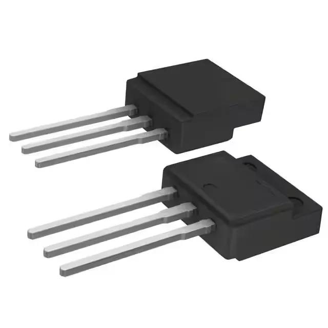
STFI11NM65N MDmesh II N-Ch MOSFET, 650V, 11A, TO-262
MPNSTFI11NM65N
Obsolete
STMicroelectronics MDmesh™ II, STFI11NM65N, N-Channel MOSFET, 650V Vdss, 11A Id, 455mOhm Rds(on) @ 10V, TO-262-3 Full Pack (I2PAKFP), Through Hole, 25W Tc power dissipation.
Independent supplier — new & surplus stockAuthenticity-screened · ESD-safe packingListing updated Jul 2026
Specifications
| Parameter | Value |
|---|---|
| Series | MDmesh™ II |
| FET type | N-Channel |
| Mounting | Through Hole |
| Drain to source voltage | 650 V |
| Drive voltage (Max rds on, min rds on) | 10V |
| Current - continuous drain (Id) @ 25°C | 11A (Tc) |
| Power dissipation | 25W (Tc) |
| Operating temperature | 150°C(TJ) |
| Package | Tube |
| Vgs | ±25V |
| Technology | MOSFET (Metal Oxide) |
| Case | TO-262-3 Full Pack, I²Pak |
| Vgs(th) (Max) @ id | 4V @ 250µA |
| Rds on (Max) @ id, vgs | 455mOhm @ 5.5A, 10V |
| Gate charge (Qg) (Max) @ vgs | 29 nC @ 10 V |
| Input capacitance (Ciss) (Max) @ vds | 800 pF @ 50 V |
Product details
Frequently asked questions
What is a suitable replacement for STFI11NM65N?
For a new design, look at current-generation 650 V N-channel MOSFETs in a through-hole Full Pack or isolated TO-220 package from ST's MDmesh series or from competitors. For a BOM fill, the closest pin-compatible alternative will share the TO-262 Full Pack (I2PAKFP) footprint and similar gate-drive voltage; parametric matching should target 650 V Vdss, 11 A Id, and 455 mΩ Rds(on) as a baseline.