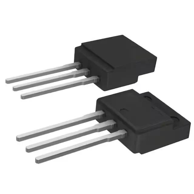
STMicroelectronics STFI10NK60Z — Discrete Semiconductors

STMicroelectronics STFI10NK60Z N-Ch MOSFET, 600 V, 10 A

MPNSTFI10NK60Z
Obsolete

STMicroelectronics SuperMESH N-Channel MOSFET, 600 V drain-source, 10 A continuous drain, 750 mOhm Rds(on) at 10 V gate drive, 70 nC gate charge, through-hole TO-262-3 full pack (I2PAKFP), -55 to 150 °C junction.

$2.4400Ref. price · indicative, final on quote
Independent supplier — new & surplus stockAuthenticity-screened · ESD-safe packingListing updated Jul 2026

Specifications

STFI10NK60Z specifications
ParameterValue
SeriesSuperMESH™
FET typeN-Channel
MountingThrough Hole
Drain to source voltage600 V
Drive voltage (Max rds on, min rds on)10V
Current - continuous drain (Id) @ 25°C10A (Tc)
Power dissipation35W (Tc)
Operating temperature-55°C~150°C(TJ)
PackageTube
Vgs±30V
TechnologyMOSFET (Metal Oxide)
CaseTO-262-3 Full Pack, I²Pak
Vgs(th) (Max) @ id4.5V @ 250µA
Rds on (Max) @ id, vgs750mOhm @ 4.5A, 10V
Gate charge (Qg) (Max) @ vgs70 nC @ 10 V
Input capacitance (Ciss) (Max) @ vds1370 pF @ 25 V

Product details

600 V, 10 A SuperMESH MOSFET — now obsolete

The STFI10NK60Z: The 750 mOhm maximum on-resistance at 4.5 A with 10 V gate drive defines the conduction loss for a given load. The 70 nC gate charge figure helps estimate switching losses and drive requirements in a typical offline flyback or PFC stage.

No last-time-buy date or official successor is recorded in the available lifecycle documentation. Date-code provenance matters here: verify the stock against the manufacturer's last production window.

The 600 V drain-source rating provides the 80 % derating margin typical for universal-input offline converters (up to 400 V bulk). The 10 A continuous current rating is the package limit at case temperature 25 °C — real-world derating applies above that, and the 35 W maximum power dissipation in the TO-262 full pack is the thermal ceiling. The 750 mOhm Rds(on) at 10 V gate drive means the conduction loss at 4.5 A drain current is roughly 15 W (I²R), which consumes nearly half the package dissipation budget — a heatsink is mandatory, and the isolated tab simplifies mounting. The 70 nC total gate charge at 10 V is moderate; a typical gate driver with 1 A source/sink capability switches this device in the tens of nanoseconds range, but the input capacitance of 1370 pF at 25 V drain-source should be considered for the drive loop layout.

Through-hole I2PAKFP — assembly and thermal notes

The three through-hole leads fit a standard TO-262 footprint.

Frequently asked questions

What is the Rds(on) of STFI10NK60Z?

The maximum on-resistance is 750 mOhm at 4.5 A drain current with 10 V gate drive. This is the figure to use for worst-case conduction loss budgeting in a flyback or PFC stage.

What is the replacement for STFI10NK60Z?

No official replacement or successor is recorded in the available lifecycle documentation. For a pin-compatible alternative, look at other SuperMESH N-channel MOSFETs in the I2PAKFP package with similar voltage and current ratings — verify the footprint and gate drive requirements against the original design. Sourcing the exact STFI10NK60Z through independent distribution remains the most direct path.