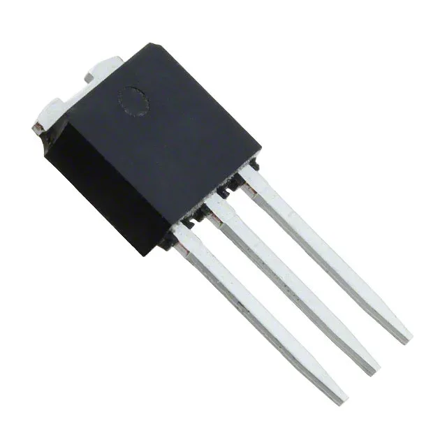
600V, 7A N-channel MOSFET in I-Pak — MDmesh™ II series
The STD8NM60N-1: The 650mΩ maximum Rds(on) at 10V gate drive and 19nC typical gate charge suit flyback, PFC boost, and two-switch forward topologies.
The 650mΩ Rds(on) at 10V Vgs and 3.5A Id is the figure to use for conduction loss calculations at full load. At 7A the dissipation in the channel alone reaches roughly 32W, which is within the 70W package limit but requires a well-designed heatsink. The 19nC gate charge at 10V is moderate — a typical gate driver with 1A peak source/sink capability will switch the device in tens of nanoseconds, keeping crossover losses manageable in hard-switched topologies. The 560pF input capacitance at 50V Vds confirms the drive requirement is modest, so a standard bootstrap or isolated gate-drive transformer can handle it.
Through-hole I-Pak — board-level mounting and thermal path
The TO-251 (I-Pak) package is a through-hole variant with three short leads and a metal tab that is soldered to the PCB for heatsinking. Unlike the surface-mount DPAK, the I-Pak's leads go through plated holes, giving a stronger mechanical bond for high-vibration environments. For the 70W maximum dissipation, a dedicated heatsink or a large copper pour on the board is necessary — the package alone cannot shed that power without a thermal interface.
Obsolete — sourcing and replacement strategy
This means STMicroelectronics has discontinued the part and no longer accepts production orders. The MDmesh™ II series has been superseded by newer generations like MDmesh™ V and MDmesh™ K5, which offer lower Rds(on) and faster switching in the same voltage class. A direct pin-compatible drop-in is not guaranteed — the replacement candidate must be evaluated for gate drive voltage, package footprint, and thermal performance. The base product number STD8N indicates the 8A current class, so a search for STD8N series devices in the same I-Pak package is a starting point.