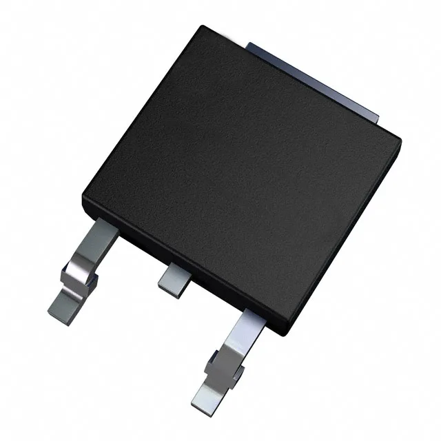
STD7N65M2

STMicroelectronics

STMicroelectronics STD7N65M2, N-channel 650 V MOSFET, MDmesh M2 series, 5 A continuous drain, 1.15 Ohm Rds(on) at 10 V, 9 nC gate charge, DPAK (TO-252) surface-mount package, -55 to 150 °C junction temperature.

STMicroelectronics STD7N65M2
Download datasheet (PDF)
[IN STOCK] In Stock: 18 pcs
$3.80/ pc

Volume pricing

Buy Now

MOQ 1 · Tape & Reel (TR) Cut Tape (CT) · RoHS · EIA-481 · DAP/DDP · T/T

Technical specifications

STD7N65M2 specifications
Parameter / AttributeSpecification / Value
SeriesMDmesh™
FET typeN-Channel
MountingSurface Mount
Drain to source voltage650 V
Drive voltage (Max rds on, min rds on)10V
Current - continuous drain (Id) @ 25°C5A (Tc)
Power dissipation60W (Tc)
Operating temperature-55°C ~ 150°C (TJ)
PackageTape & Reel (TR) Cut Tape (CT)
Vgs±25V
TechnologyMOSFET (Metal Oxide)
CaseTO-252-3, DPak (2 Leads + Tab), SC-63
Vgs(th) (Max) @ id4V @ 250µA
Rds on (Max) @ id, vgs1.15Ohm @ 2.5A, 10V
Gate charge (Qg) (Max) @ vgs9 nC @ 10 V
Input capacitance (Ciss) (Max) @ vds270 pF @ 100 V

Technical details

650 V N-channel MOSFET in DPAK — what this part is

It is built on ST's MDmesh vertical structure, which delivers a good balance of low on-resistance and fast switching for high-voltage applications.

The 650 V Vdss rating places this part in the standard high-voltage MOSFET class for offline AC-DC converters operating from rectified 230 VAC or universal mains. Input capacitance of 270 pF at 100 V drain-source is modest, keeping the switching node capacitance low for resonant or quasi-resonant topologies.

Package and mounting — DPAK (TO-252-3)

The STD7N65M2 is supplied in the DPAK (TO-252-3) surface-mount package, with two leads plus a drain tab. For the full 60 W power dissipation rating, the tab must be soldered to a sufficient copper pad area on the board, typically 1 to 2 square inches of 2 oz copper, with thermal vias to inner layers.

It is RoHS compliant per the standard STMicroelectronics declaration.

STD7N65M2
[ALLOC] verified
Quote