The STD60NF55LT4: Gate threshold voltage is 2 V max at 250 µA drain current, with a drive voltage window of 4.5 V to 10 V for achieving rated Rds(on). Total gate charge at 5 V is 56 nC — a figure that dictates the driver current needed to hit the target switching frequency without excessive cross-conduction loss. Input capacitance Ciss is 1950 pF at 25 V drain-source bias, which together with the gate charge gives a practical switching speed ceiling in hard-switched topologies. The ±15 V maximum gate-source rating provides headroom for gate-drive overshoot in noisy environments.
175°C junction — harsh-environment capability
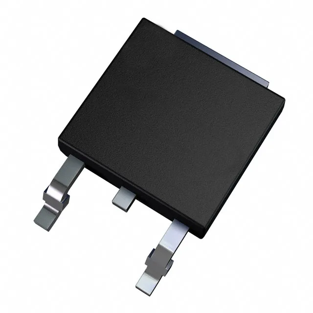
DPAK surface-mount package
The DPAK footprint is a common industry standard, easing layout reuse across multiple power MOSFET variants.