What the 500 V / 4.4 A rating means for your BOM
The STD5NK50ZT4 is an N-channel MOSFET from ST's SuperMESH™ series, built for offline flyback primaries, auxiliary power supplies, and DC-DC converters where the rail sits above 400 V. The 500 V drain-source breakdown (Vdss) gives enough headroom for universal-input flyback stages (typical reflected voltage plus leakage spike lands around 450 V).
Gate drive and switching — 10 V is the sweet spot
This part is specified with the gate driven at 10 V for the rated Rds(on). The gate threshold (Vgs(th)) max is 4.5 V at 50 µA, so a 5 V logic-level drive will turn it on but with higher on-resistance — roughly double the 1.5 Ohm. For high-efficiency switching, plan for a 10 V gate rail. Input capacitance (Ciss) is 535 pF at 25 V drain-source, a figure that helps estimate switching times and crossover losses.
Package and thermal — DPAK (TO-252) layout notes
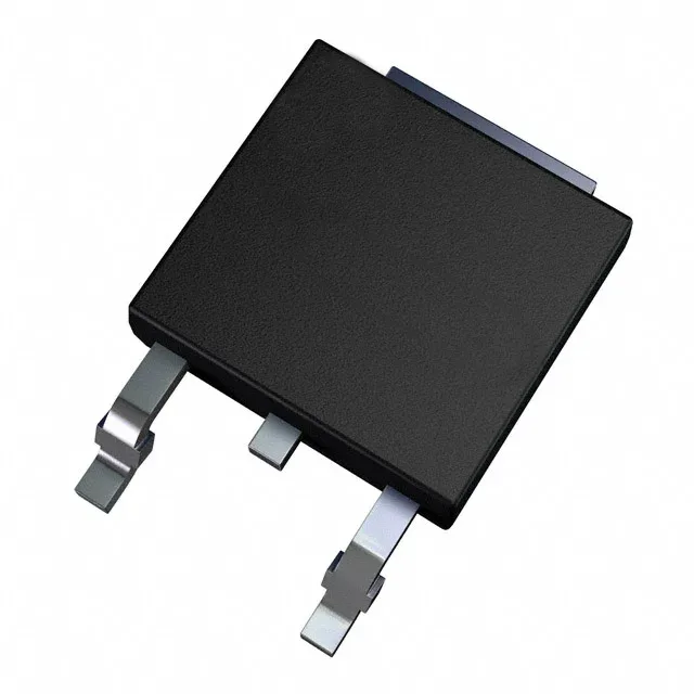
The DPAK (TO-252) surface-mount package has a metal tab that is the drain connection. The PCB footprint must include a copper pad and via stitch to the inner-layer ground plane for thermal dissipation. The 70 W power dissipation rating assumes the tab is soldered to a reasonable copper area; without that thermal path, continuous current capability drops sharply.