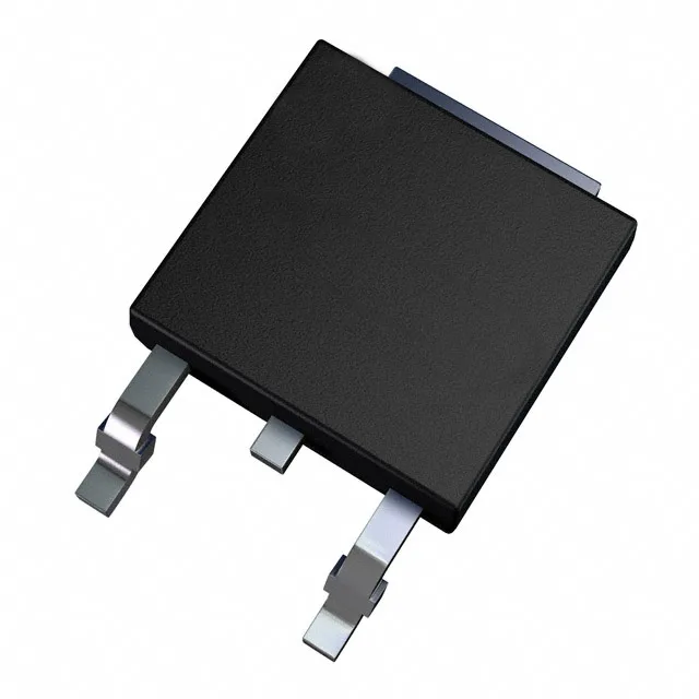
525 V N-channel MOSFET in DPAK — SuperMESH3™ series
The device is designed for high-voltage switched-mode power supplies, offline converters, and lighting ballasts where the DPAK footprint and 70 W power dissipation capability fit medium-power stages.
1.5 Ohm Rds(on) — gate drive and conduction loss
The 1.5 Ohm maximum on-resistance is specified at 2.2 A drain current with a 10 V gate-source voltage. Gate charge is 17 nC at 10 V.
This part is suitable for qualification into new production BOMs without near-term obsolescence risk. For dual-sourcing or second-source evaluation, the base product number STD5N52 identifies the family; pin-compatible alternatives within the same SuperMESH3 voltage and current class can be assessed against the specific Rds(on) and gate charge targets of the application.
Temperature range and package — mounting and environment
The DPAK (TO-252) package has a single tab that carries the drain potential; the PCB copper area and thermal vias under the tab determine the effective thermal resistance. The 70 W power dissipation rating assumes the tab is soldered to a sufficient copper land — a layout review is recommended for continuous operation above 2 A.