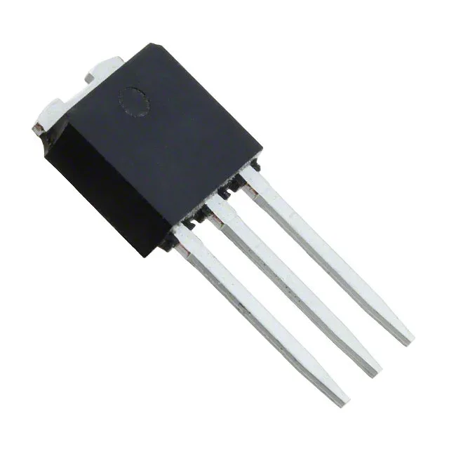
600 V N-channel MOSFET for offline flyback and auxiliary supplies
On-resistance and gate charge — the switching loss trade-off
With a maximum Rds(on) of 8 Ohm at Vgs=10 V and Id=700 mA, the conduction loss at 1 A is roughly 8 W — the designer must size the heatsink and PCB copper area to keep the junction below 150°C. Total gate charge is 10 nC at Vgs=10 V, which keeps the gate-drive energy low enough for a small-signal driver or a simple resistor-capacitor bootstrap circuit in low-frequency flyback converters. Input capacitance is 170 pF at Vds=25 V, so the switching speed is limited more by the gate-drive source impedance than by the device itself.
For new designs, consider a current-production SuperMESH™ N-channel MOSFET in a similar voltage and current class — the TO-251 (IPak) footprint is shared with several active ST parts in the same series.