Medium-voltage offline switching in a low-charge DPAK
The STD2LN60K3 is an N-channel 600 V, 2 A MOSFET from STMicroelectronics' SuperMESH3 series, built for medium-voltage offline converters and auxiliary power stages where gate-drive efficiency and thermal management in a compact surface-mount package matter more than raw current capacity. With a typical gate charge of 12 nC at 10 V and an input capacitance of 235 pF at 50 V Vds, the switching losses stay low enough that a small-signal driver can push the gate without a dedicated buffer stage — useful in flyback and PFC aux windings where every milliwatt of drive power counts.
Rds(on) and thermal budget for the real load
The 4.5 Ohm maximum on-resistance at 1 A, 10 V means that at the 2 A continuous drain rating the conduction loss hits about 18 W (I²R) before junction temperature rise — the 45 W case-temperature power dissipation limit leaves headroom only if the PCB copper area under the DPAK tab sinks the heat effectively. The 150 °C maximum junction temperature sets the derating ceiling; a real design should budget the junction rise to 125 °C or lower to stay inside the safe operating area over the full ambient range.
Package and mounting reality for the layout
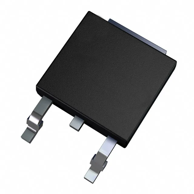
The DPAK (TO-252-3) surface-mount package with a single exposed tab requires a thermal land pattern on the PCB that connects the drain pad to a copper pour — the tab is the primary heat path, not the leads. The ±30 V maximum gate-source voltage means the gate drive must never exceed that rail, even during transients — a 12 V gate drive is safe, but a bootstrap supply that rings above 30 V during switching will punch the oxide.