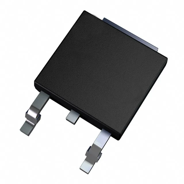
100 V, 25 A N-channel MOSFET in DPAK — what the ratings mean for the BOM line
The STD25NF10T4: Maximum on-resistance is 38 mOhm at 12.5 A drain current with a 10 V gate drive — this is the conduction loss figure to budget for in the thermal calculation at the expected load current.
Switching performance and gate drive budget
Input capacitance (Ciss) is 1550 pF at 25 V drain-source — this sets the switching speed limit and the driver's peak current requirement for fast edges.
Package, thermal, and compliance
Maximum gate-source voltage is ±20 V — the gate drive must not exceed this absolute maximum, even during transients, to avoid oxide rupture.