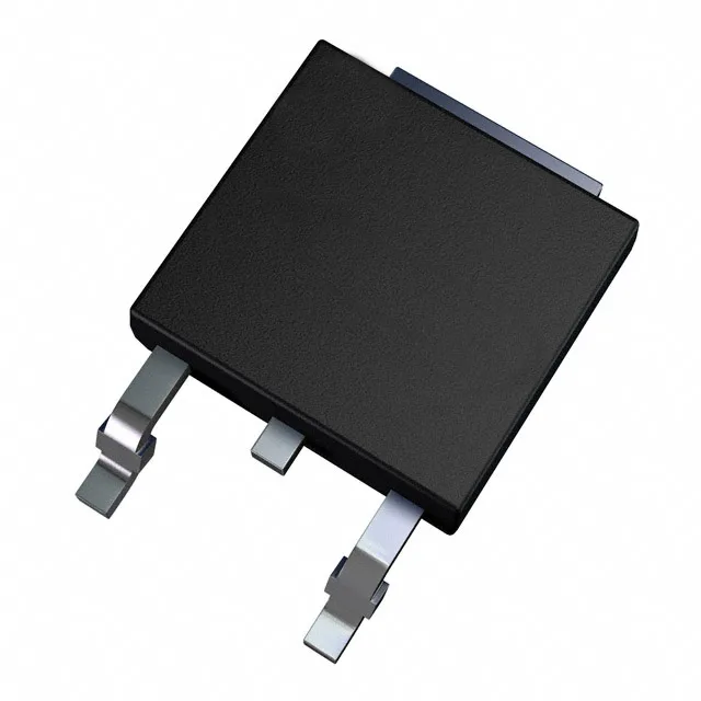
STMicroelectronics STD25N10F7 — Discrete Semiconductors

STD25N10F7 N-Channel MOSFET, 100V 25A DPAK

MPNSTD25N10F7
Active

STMicroelectronics DeepGATE™, STripFET™ VII N-Channel MOSFET, 100V, 25A, 35mOhm, DPAK, Tape & Reel.

$1.3400Ref. price · indicative, final on quote
PackagingTO-252-3, DPak (2 Leads + Tab), SC-63
RoHSROHS3 Compliant
SeriesDeepGATE™, STripFET™ VII
Independent supplier — new & surplus stockAuthenticity-screened · ESD-safe packingListing updated Aug 2026

Specifications

STD25N10F7 specifications
ParameterValue
SeriesDeepGATE™, STripFET™ VII
FET typeN-Channel
MountingSurface Mount
Drain to source voltage100 V
Drive voltage (Max rds on, min rds on)10V
Current - continuous drain (Id) @ 25°C25A (Tc)
Power dissipation40W (Tc)
Operating temperature-55°C ~ 175°C (TJ)
PackageTape & Reel (TR) Cut Tape (CT)
Vgs±20V
TechnologyMOSFET (Metal Oxide)
CaseTO-252-3, DPak (2 Leads + Tab), SC-63
Vgs(th) (Max) @ id4.5V @ 250µA
Rds on (Max) @ id, vgs35mOhm @ 12.5A, 10V
Gate charge (Qg) (Max) @ vgs14 nC @ 10 V
Input capacitance (Ciss) (Max) @ vds920 pF @ 50 V

Product details

100 V, 25 A, 35 mOhm — the switching workhorse in a DPAK

The STD25N10F7 is an N-channel MOSFET from STMicroelectronics' DeepGATE™ and STripFET™ VII series, rated for 100 V drain-source and 25 A continuous drain current at 25°C case temperature. With a maximum on-resistance of 35 mOhm at 12.5 A and 10 V gate drive, it handles moderate-power switching in DC-DC converters, motor drives, and battery-management circuits without needing a heatsink in many layouts. The DPAK (TO-252) package is a surface-mount format that reworks well with a hot-air station or a soldering iron — the exposed tab carries the drain current and needs a decent copper pour on the PCB to pull heat away. At 40 W maximum dissipation, the thermal path through the tab matters more than the package itself.

Gate charge and capacitance — what they mean for the driver

Total gate charge is 14 nC at 10 V gate drive — a modest figure that keeps the gate-driver power loss low even at switching frequencies above 100 kHz. The input capacitance is 920 pF at 50 V drain bias, which means the driver sees a light capacitive load and the switching edges stay sharp without excessive ringing. The 4.5 V maximum gate threshold at 250 µA drain current means a 5 V logic-level gate drive will turn the device on fully, but the on-resistance is specified at 10 V drive — so for lowest conduction loss, budget a 10 V gate rail. The ±20 V Vgs max gives headroom for gate overshoot in hard-switching topologies.

Frequently asked questions

Can I use STD25N10F7 as a drop-in for STB30NF10T4?

Not without checking the PCB layout. The STB30NF10T4 is a D2PAK (TO-263) part — larger footprint and higher current rating (35 A vs 25 A). The STD25N10F7 in DPAK has a smaller tab and lower power dissipation (40 W vs 115 W). If the board is laid out for a D2PAK, the DPAK will not align; a new footprint is required. Electrically, the STD25N10F7 has lower Rds(on) (35 mOhm vs 45 mOhm) and much lower gate charge (14 nC vs 55 nC), which means lower conduction and switching losses at the same current.