550 V, 16 A — the switching envelope
The STD18N55M5 is an N-channel 550 V, 16 A MOSFET from STMicroelectronics' MDmesh™ V series, built for hard-switching topologies in power supplies, adapters, and lighting ballasts.
Maximum on-resistance is 192 mOhm at 8 A drain current with 10 V gate drive — the conduction loss floor for a 2–4 A RMS load in a typical LLC or flyback primary switch. Input capacitance is 1260 pF at 100 V Vds, which sets the driver's dynamic current draw and the switching energy per cycle.
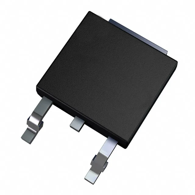
DPAK footprint and thermal layout
The TO-252-3 (DPAK) package with a single exposed drain tab requires a minimum 300–400 mm² copper area on the top layer for the 110 W dissipation to be achievable. The 10 V gate drive voltage is mandatory to reach the rated Rds(on); driving with 5 V logic leaves the FET in the linear region and risks thermal runaway.
ROHS3 compliant, with ±25 V maximum gate-source voltage and a 5 V threshold at 250 µA. The MDmesh™ V series is ST's mainstream high-voltage MOSFET platform; no official second-source cross-reference is published, but the 550 V / 16 A DPAK space has multiple contenders from Infineon, ON Semi, and Vishay for dual-sourcing qualification.