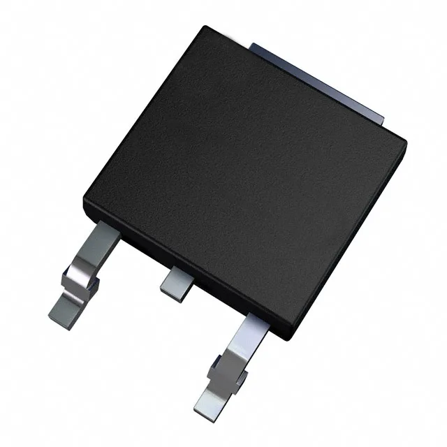
Its 150 MHz transition frequency confirms it is a switching device, not a linear amplifier — the 400 mV max Vce(sat) at 3 A keeps conduction losses within the 15 W power dissipation ceiling of the DPAK footprint. The 150°C junction temperature rating gives thermal headroom for enclosed or warm-environment designs, but the 100 nA collector cutoff at 60 V means off-state leakage is negligible for most loads.
For a BOM line that currently specifies this transistor, the immediate decision is whether to place a last-time-buy quantity to cover the remaining production run, or to qualify a pin-compatible replacement before the window closes. The base product number STD1802 covers the broader family, so a sibling variant within the same die family may still be active — verify the exact suffix against current lifecycle data before committing a last-time-buy volume.
Package and thermal reality — DPAK on a production board
The DPAK (TO-252-3, two leads plus tab) is a surface-mount power package that relies on the exposed drain tab for thermal dissipation. The 15 W power max is achievable only with adequate copper area on the PCB — a standalone footprint without a thermal via stitch under the tab will derate that number significantly. For a 3 A continuous load at 400 mV Vce(sat), the conduction loss is about 1.2 W, which is manageable with a reasonable copper pour.