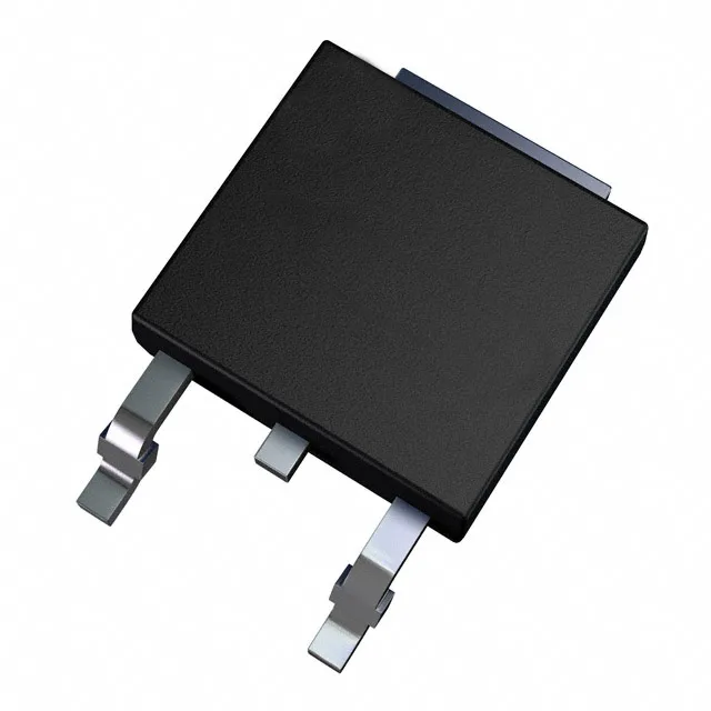
650V N-channel in DPAK — MDmesh M2 generation
The STD16N65M2 is an N-channel power MOSFET from STMicroelectronics, built on the MDmesh M2 planar technology.
Switching charge and input capacitance
Gate charge (Qg) is 19.5 nC at Vgs = 10 V, and input capacitance (Ciss) is 718 pF at Vds = 100 V. The low Qg relative to the 650 V class means the gate driver sees a light reactive load — a standard 1 A gate-driver IC can switch this FET at 100 kHz without excessive cross-conduction losses. The DPAK (TO-252-3) surface-mount package with a single tab carries the 110 W power dissipation at case temperature. The thermal path runs through the tab — the PCB copper area on the drain pad sets the real-world junction-to-ambient resistance, not the package alone.
Temperature range and drive threshold
The maximum gate threshold voltage (Vgs(th)) is 4 V at 250 µA drain current — a logic-level 5 V gate signal barely turns it on; 10 V gate drive is the practical minimum for full enhancement. Maximum gate-source voltage is ±25 V, giving tolerance to ringing on the gate node in hard-switching layouts without external clamping.
Active production — sourcing and compliance
RoHS compliance is standard for the MDmesh M2 family; specific REACH and UL documentation is available from STMicroelectronics on request.