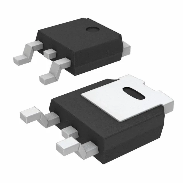
STD16N50M2

STMicroelectronics

STMicroelectronics MDmesh™ N-Channel MOSFET, 500 V Vdss, 13 A continuous drain current, 280 mOhm Rds(on) at 10 V, 19.5 nC gate charge, DPAK (TO-252) surface-mount package, -55°C to 150°C junction temperature.

STMicroelectronics STD16N50M2
Download datasheet (PDF)
[IN STOCK] In Stock: 10 pcs
$1.73/ pc

Volume pricing

Buy Now

MOQ 1 · Tape & Reel (TR) Cut Tape (CT) · RoHS · EIA-481 · DAP/DDP · T/T

Technical specifications

STD16N50M2 specifications
Parameter / AttributeSpecification / Value
SeriesMDmesh™
FET typeN-Channel
MountingSurface Mount
Drain to source voltage500 V
Drive voltage (Max rds on, min rds on)10V
Current - continuous drain (Id) @ 25°C13A (Tc)
Power dissipation110W (Tc)
Operating temperature-55°C ~ 150°C (TJ)
PackageTape & Reel (TR) Cut Tape (CT)
Vgs±25V
TechnologyMOSFET (Metal Oxide)
CaseTO-252-3, DPak (2 Leads + Tab), SC-63
Vgs(th) (Max) @ id4V @ 250µA
Rds on (Max) @ id, vgs280mOhm @ 6.5A, 10V
Gate charge (Qg) (Max) @ vgs19.5 nC @ 10 V
Input capacitance (Ciss) (Max) @ vds710 pF @ 100 V

Technical details

MDmesh™ 500 V N-channel MOSFET in DPAK

500 V blocking and 110 W dissipation — sizing the thermal budget

The 500 V Vdss rating covers the bulk-capacitor voltage in a universal-input flyback or PFC stage with healthy derating for transients. At 110 W maximum power dissipation (case temperature referenced), the junction-to-case thermal path must be kept low; the DPAK's exposed tab is the primary heat-removal route. A 280 mOhm Rds(on) at 10 V means conduction losses stay manageable at the 6.5 A test point, but at 13 A full load the I²R loss reaches 47 W — check the SOA curve and heatsinking before committing to continuous operation at the rated current.

Gate drive and switching — 19.5 nC Qg at 10 V

For production BOMs this removes the urgency to qualify a substitute, though a second-source evaluation for dual-sourcing resilience is always a prudent step.

STD16N50M2
[ALLOC] verified
Quote