100 V, 23 A N-channel in DPAK — conduction loss and thermal budget
This is a switching MOSFET, not a linear-mode device.
Gate drive and switching — 10 V logic, 40 nC Qg
The input capacitance Ciss is 870 pF typical at 25 V drain-source, which is moderate — the driver sees a capacitive load that rises as Vds falls during the Miller plateau. The maximum gate-source voltage rating is ±20 V, giving margin above the 10 V drive level. The 4 V maximum threshold at 250 µA means the FET is fully off below 4 V gate-source, which is compatible with standard 5 V logic if the gate drive is level-shifted to 10 V.
Package and board integration — DPAK footprint and thermal pad
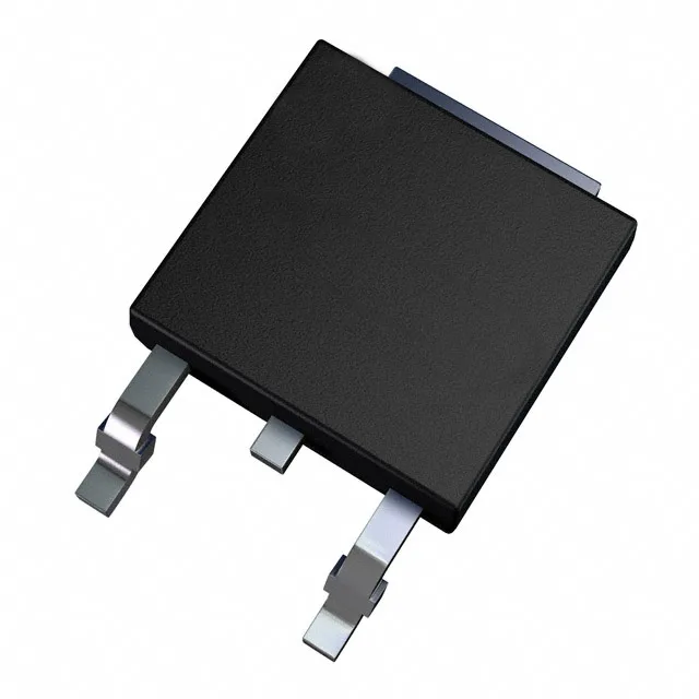
The STD15NF10T4 is supplied in the TO-252-3 DPAK package (DPak, 2 leads plus tab, SC-63). The DPAK footprint is standard — the pad area under the tab directly sets the junction-to-ambient thermal resistance. The part is surface-mount only. The listed packaging options include Tape & Reel and Cut Tape, which covers both production reel quantities and prototype or repair volumes.
The part is ROHS3 compliant. The base product number is STD15, which covers a family of 100 V N-channel MOSFETs in DPAK with varying Rds(on) and current ratings. The STD15NF10T4 is the 65 mOhm variant in the standard 10 V gate-drive version.