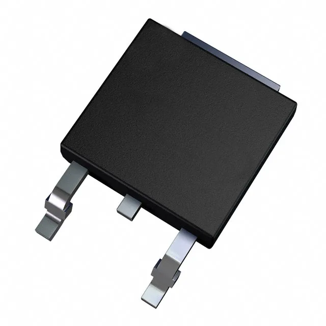
650 V N-channel — the design margin for 600 V rails
That 650 V rating puts 50 V of margin above a 600 V bus — enough headroom to absorb switching transients without avalanche stress in a typical PFC or flyback stage.
On-resistance and gate drive — the efficiency pair
That is the conduction-loss floor for the BOM — at 5.5 A the dissipation is about 10.3 W, which the DPAK package's exposed tab must sink to the board copper. Gate charge totals 22 nC at 10 V, so a standard 1 A gate driver can switch this FET at 100 kHz with about 2.2 W of drive loss — well within a typical driver's SOA.
DPAK — thermal path is the layout constraint
The DPAK (TO-252) surface-mount package has a single exposed drain tab. The datasheet's 85 W power dissipation assumes the tab is soldered to a minimum copper area on the PCB — a 2-layer board with a 1 oz pour under the tab will not hit that ceiling. For continuous operation above 30 W, a 4-layer board with thermal vias under the tab is the practical choice.