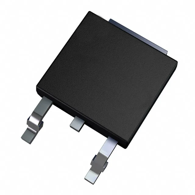
600 V N-channel in a DPAK — where the rating matters
The FDmesh™ II technology gives this part a fast-recovery body diode, which reduces reverse-recovery losses in bridge topologies like LLC resonant converters or phase-shifted full bridges — a genuine difference from older planar MOSFETs that would ring and dissipate more in that diode turn-off event.
450 mOhm on-resistance — what it costs you in copper and airflow
That works out to roughly 11 W conduction loss at 5 A — a number that drives the heatsinking decision, not just the silicon rating. The DPAK (TO-252) package has an exposed tab on the drain — the PCB copper area under that tab is the primary heatsink, so the layout engineer should allocate enough copper pour and vias to a ground plane to pull heat out.
The base product number STD11 covers a family of variants; the ND suffix indicates the FDmesh™ II version with the fast diode. If you are sourcing for a production run, this is a standard catalog item, not a niche or phased-out line.
Gate drive and switching — the 30 nC number
The maximum gate charge is 30 nC at a 10 V gate drive. That is modest — a typical gate-driver IC or a PWM controller output can charge that in a few hundred nanoseconds, keeping switching losses manageable at frequencies up to 100 kHz or so. The input capacitance is 850 pF at 50 V drain bias, which sets the drive impedance requirement for clean turn-on without ringing. The gate-source voltage is rated to ±25 V, so standard 12 V or 15 V gate drives are safe; no external clamp needed unless the drive overshoots beyond that.