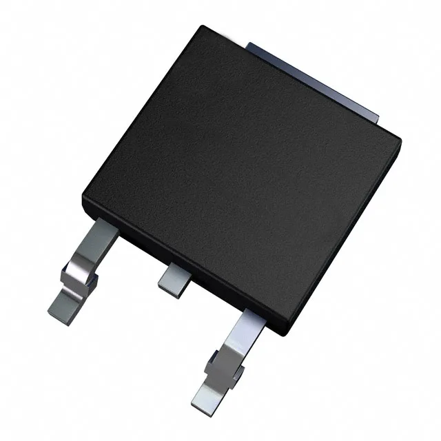
The STMicroelectronics STD10NM50N is a 500 V N-channel power MOSFET from the MDmesh™ II series. The 17 nC gate charge is specified at 10 V.
Gate drive voltage — 10 V is mandatory, not optional
This is not a logic-level MOSFET — driving it from a 5 V rail will leave the channel partially enhanced, with on-resistance roughly double the spec. Your gate-driver circuit needs a 10-12 V rail, either from a bootstrap supply or a dedicated regulator. The maximum gate-source voltage is ±25 V, so a 12 V rail with a 15 V zener clamp is safe.
Switching performance — low Qg for the voltage class
The input capacitance is 450 pF at 50 V drain-source, so the driver doesn't need to sink large peak currents. This combination of Qg and Ciss means a simple bootstrap driver IC or even a discrete push-pull stage works. The MDmesh™ II process reduces the Miller plateau, which helps with EMI — you'll see cleaner switching edges than an older planar MOSFET at the same voltage.
Thermal reality — 70 W max, but derate aggressively
The 70 W power dissipation is at case temperature 25°C, which is a lab condition. In a real enclosed power supply at 85°C ambient, the usable dissipation drops to maybe 20-25 W with a decent copper area on the DPAK tab. The 150°C maximum junction temperature gives headroom, but Rds(on) roughly doubles at 125°C junction, so conduction losses climb faster than you'd budget from the 25°C spec.
Obsolete — the sourcing picture
This means STMicroelectronics has stopped production; there is no last-time-buy window open. New designs should not use this part.