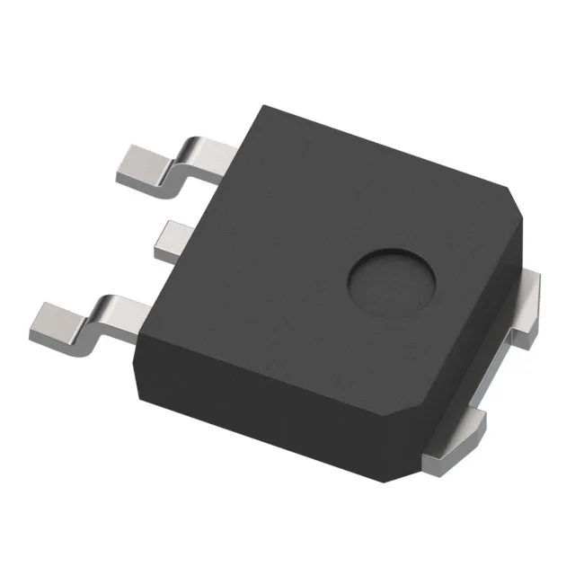
Conduction and switching parametrics for the BOM
The STD10NF30: Rds(on) is specified at 330 mOhm maximum with Id=5 A and Vgs=10 V — the drive voltage for minimum on-resistance is 10 V, so a gate driver rail at 10 V or above is needed to reach the rated Rds(on). Gate charge totals 23 nC at 10 V; input capacitance is 780 pF at 25 V drain bias — these numbers let a standard gate driver IC switch the FET at tens of kilohertz without excessive cross-conduction losses. Maximum power dissipation is 103 W at case temperature 25°C — the DPAK copper pad area on the PCB sets the actual thermal resistance; a 1-inch-square pad on a 2-oz copper board is the typical starting point for this dissipation level.
AEC-Q101 qualification is listed, which means the part has passed the automotive stress tests (HTRB, H3TRB, TC, etc.) required for Tier-1 supplier approval in powertrain, body, and chassis modules.