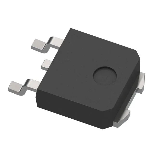
600 V N-channel MOSFET in the MDmesh M6 family
The device comes in a surface-mount DPAK (TO-252) package, which has a metal tab for heat sinking to the PCB. What sets this part apart is the MDmesh M6 technology, which delivers a low gate charge of 8.8 nC at 10 V and an on-resistance of 600 mOhm at 3.2 A, 10 V drive. This combination makes it well-suited for resonant converters, flyback power supplies, and PFC stages where switching losses matter and the board space is tight. The maximum gate-source voltage is ±25 V, and the maximum power dissipation is 60 W at the case.
At 6.4 A the on-resistance will be higher due to self-heating, so size the thermal path for the actual RMS current in your topology. Mind the dead-time if you are running this in a half-bridge; the Miller plateau is short, but the dV/dt can still couple through Cgd if the layout is loose. Input capacitance is 338 pF at 100 V drain bias, which is modest. This helps the driver turn the device on and off quickly without excessive cross-conduction loss during the switching transition.
DPAK (TO-252) — footprint and thermal reality
The DPAK (TO-252) is a surface-mount power package with three leads and a large metal tab. Without a proper via stitch under the tab, the 60 W maximum dissipation is academic — the junction will runaway well before that. Plan for a minimum 2 oz copper pour on the top layer and thermal vias to the inner or bottom ground plane if you are pulling more than a couple of amps continuous.
The base product number is STD10.