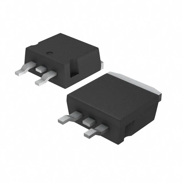
650 V, 190 mOhm — what that buys in an offline supply
That voltage class targets the primary side of offline flyback, PFC boost, and LLC resonant converters where the DC bus sits around 400 V and the drain rings past 600 V during turn-off.
For a 100 kHz hard-switched converter, the gate-drive power is Qg × Vgs × fsw = 50 nC × 10 V × 100 kHz = 50 mW — well within a standard driver's dissipation. Keep the gate-loop inductance tight; a 10 Ω series gate resistor is a typical starting point to damp ringing without slowing the edge too much.
Thermal and mounting — D2PAK real estate
Maximum power dissipation is 125 W at case temperature. A two-layer board with a 2 oz copper pad under the tab and vias to an internal plane keeps the junction below 125°C at 30–40 W dissipation. Surface-mount assembly: standard reflow profile for lead-free solder. The tab solder joint is visually inspectable from the board edge. No special moisture sensitivity level is stated, but a bake at 125°C for 24 hours before reflow is safe practice if the tape has been opened and exposed to humid shop air.