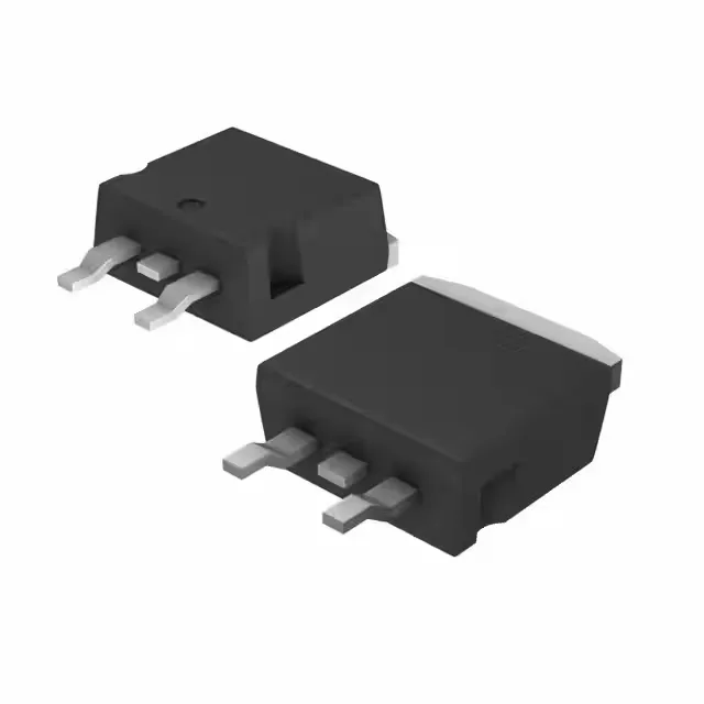
Gate drive and switching — the 56 nC number matters more than the Rds(on) in hard-switched designs
At 10 V gate drive the 56 nC gate charge is modest for a 550 V / 20 A device — it keeps the driver stage simple and the switching losses predictable in a 100 kHz PFC or flyback. The 1480 pF input capacitance at 25 V drain bias is a sanity check for the driver's peak current capability; a 1 A driver charges it in roughly 1.5 µs. The ±30 V maximum gate rating gives headroom for ringing on the gate node without an external clamp zener in most layouts.
It is ROHS3 compliant.