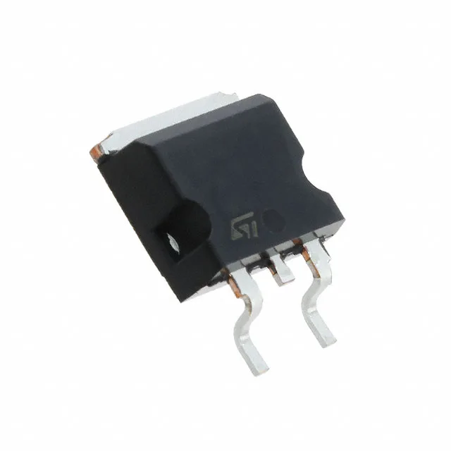
STMicroelectronics STB15N80K5

STB15N80K5 N-Channel 800V 14A MOSFET, SuperMESH5™, 375mOhm

MPNSTB15N80K5
End of Life

STMicroelectronics STB15N80K5, SuperMESH5™ N-Channel MOSFET, 800V Vdss, 14A Id, 375mOhm Rds(on) at 10V, D2PAK (TO-263), -55°C to 150°C.

$5.32Ref. price · indicative, final on quote
PackagingTO-263-3, D²Pak (2 Leads + Tab), TO-263AB
StockContact for availability
MOQ1 pcs
  • 100% new & originalTraceable channels only — no refurbs, no pulls, no remarked parts.
  • Date & lot codes on quoteStated per line before you commit; label photos on request.
  • MSL-compliant ESD packingMoisture-sealed bags with indicator cards; reels photo-verified.
  • PayPal buyer protectionPay by T/T, PayPal or Payoneer — card payments covered end to end.

Specifications

STB15N80K5 Technical Specifications
ParameterValue
SeriesSuperMESH5™
FET typeN-Channel
Mounting typeSurface Mount
Drain to source voltage800 V
Drive voltage (Max rds on, min rds on)10V
Current - continuous drain (Id) @ 25°C14A (Tc)
Power dissipation190W (Tc)
Operating temperature-55°C ~ 150°C (TJ)
PackageTape & Reel (TR); Cut Tape (CT)
Vgs±30V
TechnologyMOSFET (Metal Oxide)
CaseTO-263-3, D²Pak (2 Leads + Tab), TO-263AB
Vgs(th) (Max) @ id5V @ 100µA
Rds on (Max) @ id, vgs375mOhm @ 7A, 10V
Gate charge (Qg) (Max) @ vgs32 nC @ 10 V
Input capacitance (Ciss) (Max) @ vds1100 pF @ 100 V

Product details

800 V N-channel in D2PAK — the SuperMESH5™ switching MOSFET

The STB15N80K5 is an 800 V, 14 A N-channel power MOSFET from ST's SuperMESH5™ series, built on a strip-layout vertical DMOS process that cuts the on-resistance per unit area compared to earlier generations. Packaged in a D2PAK (TO-263) surface-mount case, it targets high-voltage switching applications where conduction loss and switching speed both matter — offline flyback converters, PFC stages, two-switch forward topologies, and LLC resonant converters in the 150–500 W range.

375 mOhm on-resistance — conduction loss floor at 7 A

This is the figure to use for worst-case conduction loss calculations at elevated junction temperature — the datasheet's typical curve shows Rds(on) roughly doubles from 25°C to 150°C, so a realistic 150°C junction pushes the effective resistance toward 750 mOhm. The 32 nC total gate charge at 10 V keeps the gate-drive energy per switching cycle low. At a 100 kHz switching frequency the average gate-drive current is about 3.2 mA, well within the capability of a standard MOSFET driver IC. The 1100 pF input capacitance at 100 V drain-source confirms the moderate switching speed — expect clean turn-on and turn-off edges with a 10–15 Ohm gate resistor to damp ringing.

190 W dissipation and the heatsink question

The 190 W maximum power dissipation at case temperature 25°C is a theoretical ceiling under ideal thermal interface — real-world dissipation is set by the junction-to-ambient thermal resistance, which for a D2PAK soldered to a typical 1 oz copper pad on a 2-layer board sits around 40–50°C/W. At 14 A continuous current with 375 mOhm Rds(on) the conduction loss alone is 73.5 W, which would push the junction above 150°C without a heatsink and forced airflow. For any continuous load above a few amps, a heatsink is mandatory. The 5 V typical gate threshold at 100 µA drain current is high enough to keep the device off during power-up transients on a 12 V gate-drive rail.

Frequently asked questions

What is the exact RDS(on) of STB15N80K5 at 10V and 7A?

This is a maximum limit at 25°C junction temperature; the typical value is lower, and the resistance increases with temperature.

Does STB15N80K5 require a heatsink for a 14A continuous current?

Yes. Without a heatsink and forced airflow, the junction temperature will exceed the 150°C maximum rating. A properly sized heatsink is required for any continuous load above a few amps.