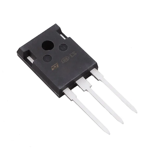
STMicroelectronics SCTWA30N120

STMicro SCTWA30N120 SiC MOSFET, 1200 V, 100 mOhm, TO-247-3

MPNSCTWA30N120
End of Life

STMicroelectronics SCTWA30N120 SiCFET, N-Channel, 1200 V drain-source, 100 mOhm Rds(on) at 20 A, 45 A continuous, 105 nC gate charge, TO-247-3 through-hole, -55 to 200 °C junction.

$30.19Ref. price · indicative, final on quote
PackagingTO-247-3
StockContact for availability
MOQ1 pcs
  • 100% new & originalTraceable channels only — no refurbs, no pulls, no remarked parts.
  • Date & lot codes on quoteStated per line before you commit; label photos on request.
  • MSL-compliant ESD packingMoisture-sealed bags with indicator cards; reels photo-verified.
  • PayPal buyer protectionPay by T/T, PayPal or Payoneer — card payments covered end to end.

Specifications

SCTWA30N120 Technical Specifications
ParameterValue
FET typeN-Channel
Mounting typeThrough Hole
Drain to source voltage1200 V
Drive voltage (Max rds on, min rds on)20V
Current - continuous drain (Id) @ 25°C45A (Tc)
Power dissipation270W (Tc)
Operating temperature-55°C ~ 200°C (TJ)
PackageTube
Vgs+25V, -10V
TechnologySiCFET (Silicon Carbide)
CaseTO-247-3
Vgs(th) (Max) @ id3.5V @ 1mA (Typ)
Rds on (Max) @ id, vgs100mOhm @ 20A, 20V
Gate charge (Qg) (Max) @ vgs105 nC @ 20 V
Input capacitance (Ciss) (Max) @ vds1700 pF @ 400 V

Product details

The STMicroelectronics SCTWA30N120 is a 1200 V N-channel silicon-carbide power MOSFET in a TO-247-3 through-hole package. It is designed for high-efficiency switching in applications such as solar inverters, EV charging, and industrial power supplies where the 1200 V drain-source rating gives headroom on a 600–800 V DC bus. The 100 mOhm on-resistance at 20 A and 20 V gate drive sets the conduction loss floor — at 20 A the dissipation is 40 W, which the 270 W package power rating can handle with adequate heatsinking. Gate charge of 105 nC at 20 V is moderate for a 1200 V SiC part; a gate driver delivering 2 A peak can switch it in under 100 ns, keeping switching losses manageable at frequencies up to 100 kHz.

Junction temperature range and package — design-in checklist

The -55°C to 200°C junction temperature range qualifies the SCTWA30N120 for high-reliability environments — avionics, downhole drilling, and outdoor telecom where the ambient can exceed 85°C and the junction sees repetitive thermal cycling. The TO-247-3 package with HiP247 Long Leads is a standard through-hole footprint — the long leads ease insertion into thick PCB or bus-bar assemblies, and the tab is the drain, so the heatsink pad is at drain potential. Input capacitance is 1700 pF at 400 V drain-source — this is the Ciss the driver sees; the low value relative to the current rating means the driver's peak current requirement stays moderate, but the gate loop inductance must be kept under 10 nH to avoid ringing.

No official second-source or pin-compatible alternate is listed in the component record — the TO-247-3 SiC MOSFET market includes parts from Wolfspeed and Rohm, but pin-compatibility should be verified against the specific gate-drive and mounting-hole layout.

Frequently asked questions

What is the Rds(on) of SCTWA30N120?

The on-resistance is 100 mOhm maximum at 20 A drain current and 20 V gate drive. This is the value to use for conduction-loss calculations at rated current.

What is the typical gate charge of SCTWA30N120?

The gate charge is 105 nC at 20 V gate drive. This total Qg determines the gate-driver power and switching speed — a 2 A driver can switch it in under 100 ns.

What is the closest pin-compatible alternative to SCTWA30N120?

The TO-247-3 SiC MOSFET market includes parts from Wolfspeed and Rohm, but pin-compatibility must be verified against the specific gate-drive and mounting-hole layout.