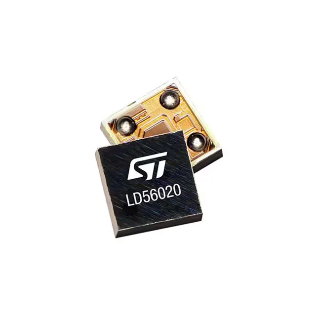
200 mA LDO in a 0.69 mm flip-chip package
The STMicroelectronics LD56020J110R is a 200 mA low-dropout linear regulator with a fixed 1.1 V output, packaged in a 4-XFBGA (4-FlipChip) measuring just 0.69x0.69 mm. This footprint is designed for space-constrained portable and battery-powered equipment where board real estate is the primary constraint — the die sits directly on the PCB with no leadframe overhead. Input voltage range extends to 5.5 V, making it suitable for single-cell Li-Ion or 3.3 V/5 V rails, while the 25 µA quiescent current keeps the regulator's own draw well below the self-discharge rate of a typical 100 mAh coin cell in always-on sensor nodes.
PSRR across the frequency band — what 90 dB to 55 dB means for noise-sensitive rails
The LD56020J110R delivers 90 dB of power-supply rejection at 100 Hz, tapering to 55 dB at 100 kHz. This is the critical band for switching-regulator ripple (typically 100 kHz to 1 MHz fundamental) and 50/60 Hz mains hum. At 100 kHz, the 55 dB rejection means that a 10 mVpp ripple on the input rail is attenuated to roughly 18 µVpp at the output — clean enough to feed an analog front-end or RF oscillator without additional post-filtering.
Thermal and protection envelope
At 125°C junction, the silicon's leakage current rises — but the 25 µA quiescent spec is measured at 25°C; expect it to roughly double at 85°C and quadruple at 125°C, still manageable for a 200 mA output stage. Built-in over-temperature and short-circuit protection shut down the regulator before the die exceeds its abs-max rating. The enable pin allows the system to gate the output rail, dropping Iq to near-zero in sleep mode.
The 4-XFBGA package (0.69x0.69 mm) has four bumps — input, output, ground, and enable. A solid ground plane under the package with at least two thermal vias to an inner-layer copper pour is recommended to keep RthJA below 150°C/W for full 200 mA output at high ambient.