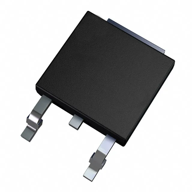
Adjustable LDO for post-regulation and point-of-load rails
The LD1117DTC-R is an adjustable positive LDO from STMicroelectronics, delivering up to 800 mA output current with a maximum dropout voltage of 1.3 V at full load. Output voltage is set with an external resistor divider from a 1.25 V reference minimum up to 15 V maximum, matching the input ceiling. The single regulator channel is internally compensated and requires only an output capacitor for stability.
Dropout headroom and quiescent current at 800 mA
At 800 mA load, the dropout voltage maxes at 1.3 V — meaning a 5 V input rail must stay above 4.3 V to hold a 3.0 V output. The quiescent current is 5 mA, typical for a medium-current LDO of this generation; it is not a low-Iq part for always-on battery applications. Compared to the LDFPVR (62 dB to 55 dB PSRR over 120 Hz to 100 kHz), the LD1117DTC-R offers better ripple rejection at line frequency but lacks the enable and power-good control features of the LDFP family. For a fixed-output low-current rail, the LD39020DTPU33R delivers 80 dB PSRR at 1 kHz but only 200 mA and a fixed 3.3 V output.
Active production in DPAK with overcurrent and overtemperature protection
On-chip protection includes overcurrent and overtemperature shutdown, covering the two most common failure modes in a linear regulator: a shorted load or a blocked heatsink path.
DPAK footprint and thermal pad considerations
The DPAK (TO-252) package exposes a large copper tab on the bottom — the tab is the output (Vout) node and the primary thermal path. Because the output is adjustable, the feedback resistor divider should be placed close to the ADJ pin to minimise noise pickup. The 1.25 V reference voltage is the lower bound; the upper bound is set by the 15 V maximum input rating minus dropout.