35 ns reverse recovery — what it buys you
In a 50 kHz or 100 kHz flyback secondary, that 35 ns trr keeps the reverse-recovery current spike short enough that the snubber and the MOSFET do not see an extra dissipation cycle. The 35 ns figure is the maximum over temperature, so the design margin stays intact across the junction range up to 150°C.
3 A average, 200 V — the continuous rating envelope
Rated for 3 A average rectified current and 200 V reverse voltage. The forward voltage drop is 1.2 V maximum at 9 A pulsed — that is the surge condition, not the continuous operating point. At 3 A the Vf will be lower, but the absolute-max table is the design boundary; stay inside it. The 10 µA reverse leakage at 200 V is a room-temperature figure; expect leakage to rise with junction temperature, so the thermal design should keep the junction below the 150°C maximum.
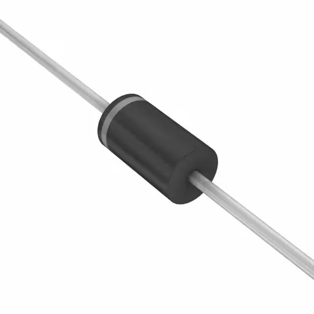
DO-201AD axial — legacy through-hole footprint
The DO-201AD axial-lead package is a through-hole form factor that has been in production for decades. It is a direct drop-in for any board originally laid out for a DO-201AD rectifier. The axial leads are crimped and soldered into plated-through holes; the body length and diameter match the standard DO-201AD cavity. If the BOM calls for a surface-mount alternative, a DO-214AB (SMC) or SMA package would require a different footprint and thermal pad design.
For a production run, the buyer should evaluate a pin-compatible fast-recovery rectifier in the same DO-201AD package with matching 200 V / 3 A / 35 ns ratings.