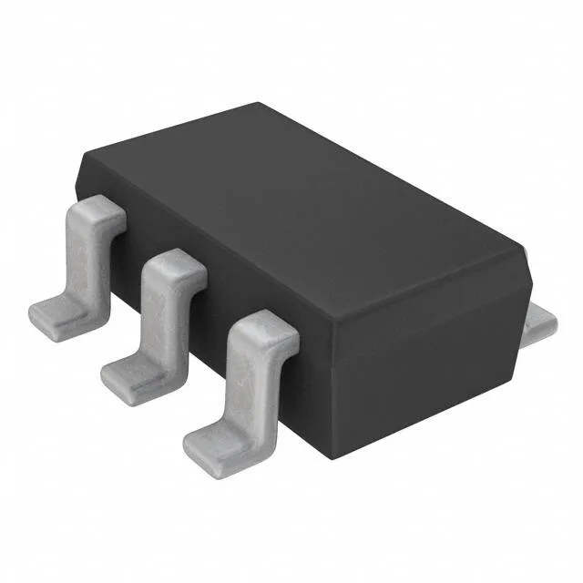
ROHM Semiconductor QSX8TR — Memory (DRAM / SRAM / Flash / EEPROM)

QSX8TR Dual NPN Transistor, 30V 1A, 320MHz, TSOT-23-6

MPNQSX8TR
End of Life

ROHM QSX8TR dual NPN transistor, 30V Vceo, 1A Ic, 320MHz fT, hFE 270 min @ 100mA, 1.25W, SOT-23-6 Thin / TSOT-23-6, Surface Mount.

$0.65Ref. price · indicative, final on quote
PackagingSOT-23-6 Thin, TSOT-23-6
StockContact for availability
MOQ1 pcs
  • 100% new & originalTraceable channels only — no refurbs, no pulls, no remarked parts.
  • Date & lot codes on quoteStated per line before you commit; label photos on request.
  • MSL-compliant ESD packingMoisture-sealed bags with indicator cards; reels photo-verified.
  • PayPal buyer protectionPay by T/T, PayPal or Payoneer — card payments covered end to end.

Specifications

QSX8TR Technical Specifications
ParameterValue
Mounting typeSurface Mount
FET type2 NPN (Dual)
Voltage - collector emitter breakdown30V
Current - collector (Ic)1A
Current - collector cutoff100nA (ICBO)
DC current gain (hFE) (Min) @ ic, vce270 @ 100mA, 2V
Power - max1.25W
Frequency320MHz
Operating temperature150°C (TJ)
PackageTape & Reel (TR); Cut Tape (CT)
CaseSOT-23-6 Thin, TSOT-23-6
Vce saturation (Max) @ ib, ic350mV @ 25mA, 500mA

Product details

Dual NPN in a compact TSOT-23-6 — what the ratings tell you

The ROHM QSX8TR is a dual NPN transistor in a TSOT-23-6 package, rated for 30V collector-emitter breakdown and 1A continuous collector current. With a minimum DC current gain of 270 at 100 mA collector current and 2V Vce, it offers high beta for low-base-current drive — useful when the upstream driver is a 3.3V or 5V logic output with limited sourcing capability. The 320 MHz transition frequency marks it as a fast-switching device suited for DC-DC converter drive, signal-level translation, or pre-driver stages where the dual die saves board area versus two discrete SOT-23s.

1.25W in a small footprint — thermal reality

The 1.25W maximum power dissipation in the TSOT-23-6 package means the junction-to-ambient thermal path is constrained. At 1A continuous switching, the Vce(sat) of 350 mV at 500 mA gives a rough dissipation of 175 mW per transistor at that point — within the package limit with margin. But if you push both transistors near 1A simultaneously at high duty cycle, the 1.25W ceiling gets tight. The 150°C junction temperature rating is the hard stop; derate the load if the board sees ambient above 85°C. A quick thermal calculation on the combined dissipation against the package rating is the right check before committing the layout.

Frequently asked questions

What is the hFE of the QSX8TR?

The minimum DC current gain (hFE) is 270 at a collector current of 100 mA and Vce of 2V. This high beta means the base drive current can be kept low — typically under 1 mA for switching loads in the 100 mA range.