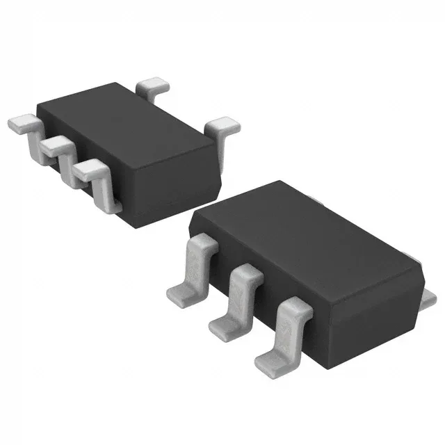
Emitter-coupled NPN/PNP pair in a thin SOT-23-5
The ROHM Semiconductor QS5Y1TR is a dual transistor — one NPN and one PNP die in a single SOT-23-5 Thin / TSOT-23-5 package, with the emitters internally connected. The transition frequency is 300 MHz for the NPN side and 270 MHz for the PNP side. This part is intended for general-purpose switching and amplification where a complementary pair is needed in a small footprint.
The 30 V Vceo sets the maximum supply rail you can connect across the collector-emitter terminals. A 24 V industrial bus is comfortable; a 48 V telecom rail is not. The 3 A collector current rating is the continuous limit per die — but at 30 V and 3 A the die dissipates 90 W, far above the 1.25 W package limit, so real-world DC current at 30 V will be derated to roughly 40 mA. The part is better suited to pulsed or saturated switching where the average power stays under the 1.25 W ceiling. Saturation voltage is specified at 400 mV maximum when driven with 50 mA base current into a 1 A collector load — a forced beta of 20, which is typical for a saturated switch. The minimum DC current gain is 200 at 500 mA, 2 V, so the part has plenty of headroom in the linear region for pre-driver stages.
Package and mounting details
The QS5Y1TR is supplied in a TSMT5 package (the supplier device package designation), which is the thin SOT-23-5 variant. It is a surface-mount device. The shipping options are Tape & Reel or Cut Tape.
It is RoHS3 compliant (2015/863/EU), free of the ten restricted substances including the four phthalates.