Automotive buck converter with 40V input tolerance
The BD9P205MUF-CE2 is a ROHM Automotive-grade step-down buck converter rated for 2A continuous output. Its 3.5V to 40V input range covers nominal 12V/24V automotive rails plus load-dump transients without external clamping — the internal FET's abs-max rating handles the surge. The synchronous rectifier keeps efficiency above 90% across most of the load range, reducing thermal stress in sealed enclosures.
Switching frequency and output flexibility
Fixed 2.2MHz switching frequency pushes the fundamental and its harmonics above the AM radio band, simplifying EMI filter design. Output voltage is adjustable from 0.8V up to 8.5V via an external resistor divider. The 0.8V reference enables powering modern 1.2V/1.8V core rails directly, while the 8.5V ceiling covers 5V and 3.3V system rails plus sensor bias supplies. Single-output positive configuration with a single feedback pin keeps the BOM simple. ROHM's Nano Pulse Control technology delivers low output ripple across the load range — the switching edge shaping reduces high-frequency ringing that couples into adjacent analog circuits. This matters when the same PCB carries sensitive ADCs or CAN transceivers sharing the battery rail.
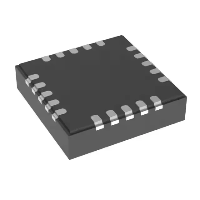
The VQFN20FV4040 package (20-lead VFQFN with exposed pad, 4 mm × 4 mm) uses wettable-flank terminations — the side-plated terminals allow automated optical inspection (AOI) of solder joints after reflow, a requirement for automotive PPAP submissions. The exposed pad must be soldered to the PCB ground plane for thermal dissipation; the datasheet's recommended footprint includes a 3.6 mm × 3.6 mm thermal pad with nine vias to the inner-layer copper. Surface-mount assembly with Tape & Reel or Cut Tape packaging options.