Buck-boost regulator with synchronous rectification
The BD83070GWL-E2: The ROHM BD83070GWL- is a single-output buck-boost regulator that steps up or steps down from a 2V to 5.5V input to deliver a fixed 2.5V or 3.3V output at up to 1A. The 1.5MHz switching frequency keeps the external inductor and capacitors small, which matters when board space is tight and the bill of materials needs to fit within a 12-ball UCSP50L1C footprint. The integrated synchronous rectifier eliminates the external Schottky diode that a non-synchronous buck-boost would need, saving a component and reducing the overall conduction loss in the power stage. For a 1A rail, that diode drop would add roughly 0.4V × 1A = 400 mW of heat that the synchronous FET instead handles internally.
Input range and output options
The 2V minimum input means the regulator can start from a single Li-ion cell near its end-of-discharge voltage (2.7V to 3.0V) and still regulate the output. The 5.5V maximum input covers the full charge voltage of a Li-ion cell at 4.2V plus margin, so the part suits battery-powered portable equipment where the rail must stay stable as the battery drains. Output is fixed at either 2.5V or 3.3V — no external resistor divider is needed. The 3.3V option is the standard logic and I/O rail for many MCUs and sensors; the 2.5V option suits lower-voltage core supplies or DDR memory termination rails in compact designs. The 1A continuous output current is the headline rating at room temperature; the actual deliverable current depends on the input-to-output voltage differential and the thermal environment. In a typical 3.3V output from a 3.7V Li-ion battery, the converter operates in buck mode with good efficiency, and the 1A rating is realistic across most of the battery discharge curve.
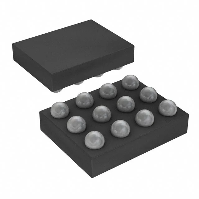
The UCSP50L1C is a 12-ball wafer-level chip-scale package (WLCSP) with a 0.5mm ball pitch. The small footprint — roughly 2.0mm × 1.5mm — suits space-constrained designs like wearables, IoT modules, or portable medical devices where every square millimeter counts. The CSPBGA alternative designation (12-UFBGA, CSPBGA) refers to the same physical package. Surface-mount assembly requires standard lead-free reflow profiles compatible with the ROHS3 compliance. The package does not have an exposed thermal pad; heat dissipation relies on the PCB copper planes and the thermal vias under the device.