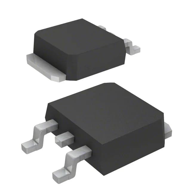
500 V N-channel switch in a DPak footprint
The RJK5033DPD-00#J2: It comes in a TO-252-3 (DPak) surface-mount package, a common footprint for mid-power switching and linear applications where the tab is soldered to a copper island for heatsinking.
On-resistance and drive voltage
The gate is rated to ±30 V, giving margin above the 10 V drive level for overvoltage transients on the gate line.
Thermal and capacitive profile
Maximum power dissipation is 65 W at the case temperature, with a 150°C maximum junction temperature. Input capacitance is 600 pF at 25 V drain-source — a moderate figure that keeps gate-drive energy low for switching frequencies in the tens of kilohertz.
Lifecycle and compliance
ROHS3 compliant, which covers the full RoHS exemption list including lead in high-melting-temperature solders.