2 GHz fanout buffer with multiplexer — what it does on the board
The Renesas 8SLVP1204ANLGI8 is a 2:4 fanout buffer with an integrated 2:1 multiplexer on the input side, meaning you can select between two differential clock sources and distribute one clean LVPECL copy to four destinations. It handles clock rates up to 2 GHz, which covers 10GbE reference clocks, SONET/SDH line cards, and high-speed ADC/DAC sampling clocks. The input stage accepts CML, LVDS, or LVPECL levels, so it can sit behind a PLL, an oscillator, or a serializer without needing a level translator.
Package and rework — 16-VFQFN with exposed pad
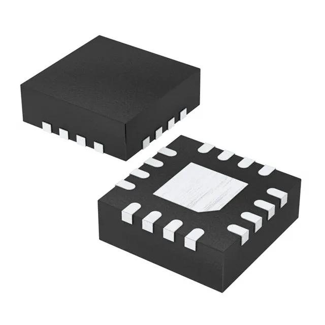
Housed in a 16-VFQFN measuring 3x3 mm, the exposed pad is the thermal path and the ground return. The exposed pad needs a via-in-pad or thermal via cluster under the center land.
Renesas lists the 8SLVP1204ANLGI8 as Active and ROHS3 compliant.