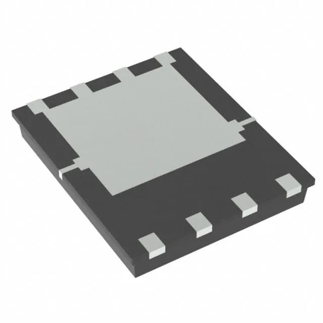
150 V N-Channel MOSFET in a 5x6 WPAK(3F) package
It is built on a standard metal-oxide semiconductor process and comes in an 8-PowerVDFN package — the WPAK(3F) variant with a 5x6 mm footprint and an exposed thermal pad for heat sinking into the PCB. Gate charge totals 37 nC at 10 V, and input capacitance is 2200 pF at 25 V drain-source — numbers that matter for the gate-driver sizing and switching-loss calculation in a 48 V or 72 V bus converter.
The 150 V drain-source rating gives headroom for 48 V and 72 V nominal rails — a 48 V bus sees transients up to 60 V, so the 150 V ceiling leaves margin without oversizing to a 200 V device. The 25 A continuous rating at 25°C case is the headline number, but the real-world current is limited by the 65 W power dissipation ceiling and the PCB's ability to sink heat from the exposed pad. Derate for ambient temperature and switching losses. The 48 mOhm Rds(on) at 10 V gate drive means conduction loss at 12.5 A is about 7.5 W — well within the 65 W dissipation limit at 25°C case, but junction temperature rise will cut into that margin at higher ambient. The 37 nC gate charge is moderate; a typical gate driver with 1 A peak source/sink can switch this FET in the 100–200 kHz range without excessive crossover loss.
Package and footprint for layout
The 8-PowerVDFN (WPAK(3F) 5x6) package is a surface-mount power package with an exposed pad on the bottom. The 5x6 mm pad needs a thermal land pattern with multiple vias to the inner ground plane — the datasheet's recommended footprint is the starting point, and the via count and copper area set the effective RthJA. The part ships in Tape & Reel, which is the standard format for automated pick-and-place assembly.