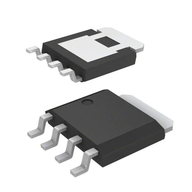
100V N-Channel MOSFET in LFPAK — active production, no LTB shadow
It's built on standard metal-oxide technology and housed in the LFPAK (SC-100, SOT-669) surface-mount package. This is a current-production part, not a phase-out line.
Maximum on-resistance is 22 mOhm at a 10 A drain current with 10 V gate drive. That's the Rds(on) ceiling for conduction-loss calculations at 25°C junction; expect the typical value to be lower, and the curve to climb with temperature. Gate charge totals 27 nC at 10 V. Combined with the 2000 pF input capacitance at 10 V drain-source, the FET needs roughly 0.5 µC per switching cycle — manageable for a standard 1-2 A gate driver at 100-200 kHz. Power dissipation is capped at 55 W at the case. That's the thermal anchor for heatsink sizing: at 20 A the conduction loss alone is 8.8 W (I² × Rds(on)), well within the 55 W budget, but switching losses and ambient derating eat into the margin.
10 V gate drive — standard logic, no special driver needed
The drive voltage for achieving the rated Rds(on) is 10 V. Junction temperature rating is 150°C. That's the absolute maximum for the silicon; continuous operation at full 20 A load will push the die temperature toward that limit without adequate heatsinking or airflow.