Gate charge and switching speed — 35 nC at 10 V
Total gate charge is 35 nC at 10 V, which means a standard gate driver (1–2 A peak) can switch this FET in the tens-of-nanoseconds range without excessive drive power. The 2550 pF input capacitance at 10 V drain-source is typical for this current class — plan your gate-drive loop inductance accordingly to avoid ringing. Maximum gate-source voltage is ±20 V, so the 10 V drive used for the Rds(on) spec is well inside the safe window; no need for a zener clamp unless the gate driver overshoots.
Thermal and power — 60 W dissipation, 150 °C junction
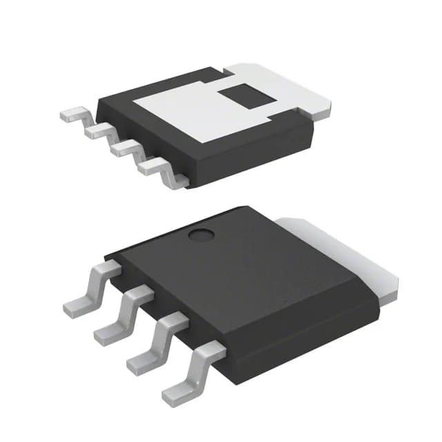
Maximum power dissipation is 60 W at case temperature, and the junction is rated to 150 °C. In a real board, the LFPAK's exposed pad soldered to a 1 oz copper plane of at least 2–3 square inches on the top layer will keep the junction below 125 °C at 30 A continuous — but derate above 25 °C ambient per the datasheet curve.
Active production, ROHS3 compliant
ROHS3 compliant, no exemptions needed for lead-free assembly.