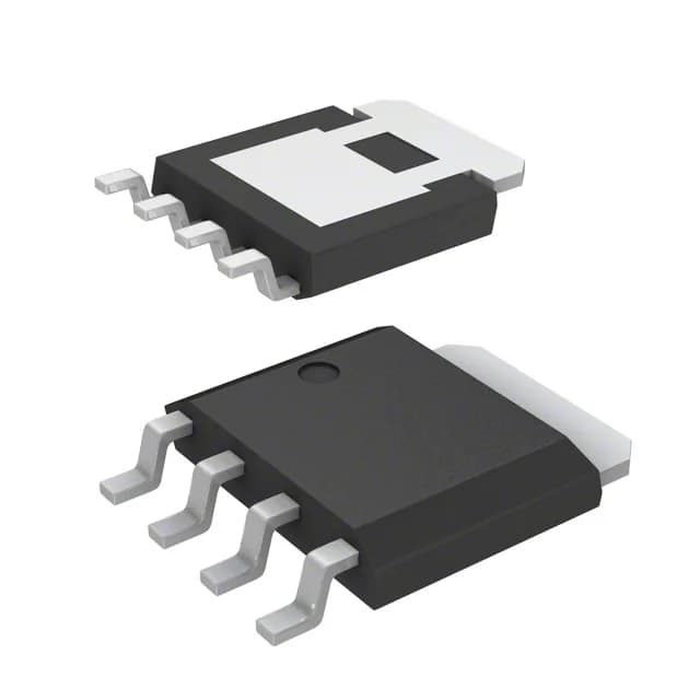
80 V, 30 A N-channel in LFPAK — switching-loss profile
The LFPAK (SOT-669) package keeps the source inductance low, which matters for the switching loop in a hard-switched converter.
Gate drive and switching budget
Gate charge is 28 nC maximum at 4.5 V, and the drive voltage range spans 4.5 V to 10 V for minimum on-resistance. A 5 V logic-level gate driver can switch this MOSFET without a separate boost stage, which simplifies the gate-drive supply in a 12 V input DC-DC converter. Input capacitance is 4150 pF at 10 V drain-source — the driver must source that charge per switching cycle. Maximum power dissipation is 55 W at the case temperature, with the junction rated to 150 °C.