Gate charge and switching — sizing the driver
Total gate charge is 35 nC at 10 V. That is a moderate figure — a standard gate driver delivering 1 A peak can switch this FET in the tens of nanoseconds. The input capacitance of 2550 pF at 10 V drain is consistent with a device optimised for hard-switching in the 100–500 kHz range.
Package and thermal — the LFPAK footprint matters
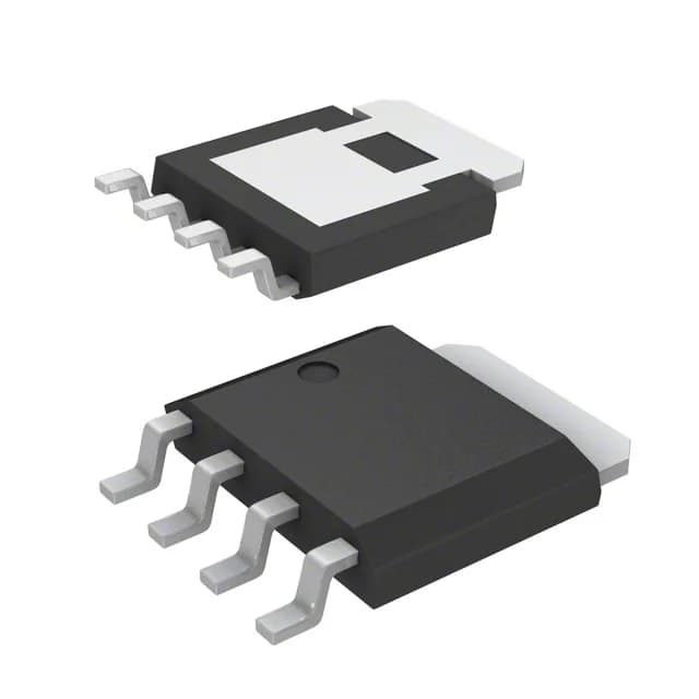
The LFPAK (SC-100, SOT-669) is a surface-mount package with an exposed drain pad. Rated for 60 W dissipation at the case, the real thermal performance depends on the PCB copper area and via count under the pad. A 4-layer board with thermal vias to an inner ground plane is the standard approach to keep the junction below 150 °C at full load.