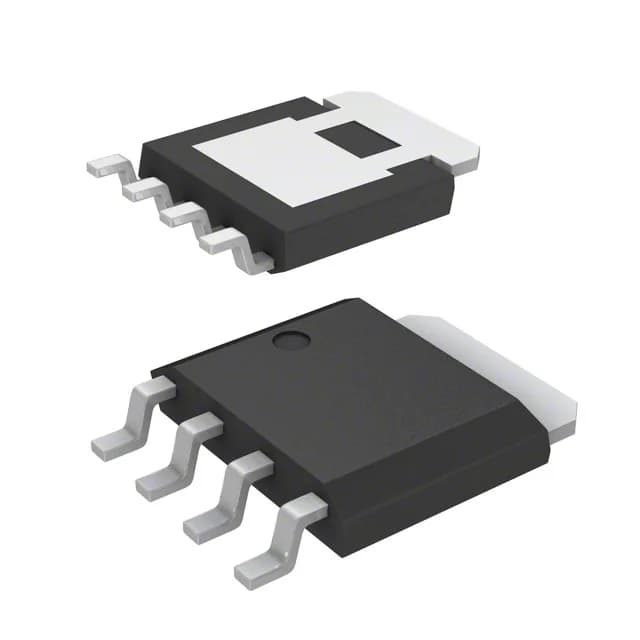
Renesas Electronics RJK0455DPB-00#J5

RJK0455DPB-00#J5 N-Channel MOSFET, 40 V, 45 A, LFPAK

MPNRJK0455DPB-00#J5
End of Life

Renesas RJK0455DPB-00#J5 N-Channel MOSFET, 40 V drain-to-source voltage, 45 A continuous drain current at 25 °C, 3.8 mOhm Rds(on) at 22.5 A, 10 V, LFPAK (SC-100, SOT-669) surface-mount package.

$2.71Ref. price · indicative, final on quote
PackagingSC-100, SOT-669
StockContact for availability
MOQ1 pcs
  • 100% new & originalTraceable channels only — no refurbs, no pulls, no remarked parts.
  • Date & lot codes on quoteStated per line before you commit; label photos on request.
  • MSL-compliant ESD packingMoisture-sealed bags with indicator cards; reels photo-verified.
  • PayPal buyer protectionPay by T/T, PayPal or Payoneer — card payments covered end to end.

Specifications

RJK0455DPB-00#J5 Technical Specifications
ParameterValue
FET typeN-Channel
Mounting typeSurface Mount
Drain to source voltage40 V
Drive voltage (Max rds on, min rds on)10V
Current - continuous drain (Id) @ 25°C45A (Ta)
Power dissipation60W (Tc)
Operating temperature150°C (TJ)
PackageTape & Reel (TR); Cut Tape (CT)
Vgs±20V
TechnologyMOSFET (Metal Oxide)
CaseSC-100, SOT-669
Rds on (Max) @ id, vgs3.8mOhm @ 22.5A, 10V
Gate charge (Qg) (Max) @ vgs34 nC @ 10 V
Input capacitance (Ciss) (Max) @ vds2550 pF @ 10 V

Product details

ROHS3 compliant per the listing, so no conflict with EU or global RoHS directives. No special handling or exemption paperwork needed for the BOM.

40 V, 45 A — the load budget anchor

For a 12 V or 24 V rail, that leaves healthy derating margin — the 40 V Vdss covers transients on a 24 V bus without avalanche worry. The 45 A rating sets the load budget: a motor-drive or DC-DC stage pulling 30 A continuous is well inside the SOA at 25 °C case. On-resistance is 3.8 mOhm maximum at 22.5 A, 10 V gate drive. That is the conduction loss floor — at 30 A, I²R loss is about 3.4 W, well within the 60 W power dissipation ceiling at case temperature Tc.

Gate charge and switching — what the 34 nC means

Total gate charge Qg is 34 nC at 10 V. For a 100 kHz switching frequency, the average gate-drive current needed is Qg × f = 3.4 mA — a standard driver handles that easily. At 500 kHz the drive current climbs to 17 mA, still within most gate-drive ICs, but the input capacitance Ciss of 2550 pF at 10 V means the driver must source enough peak current to charge that capacitance quickly for clean edges. At 60 W dissipation, the junction-to-case thermal path is the bottleneck.

LFPAK — footprint and thermal reality

The SC-100 / SOT-669 LFPAK package is a 5×6 mm surface-mount power package with an exposed drain pad. Without adequate thermal vias to an inner-layer plane, the 60 W power dissipation rating is unreachable. Surface-mount only; no through-hole variant. The 0.50 mm pitch leads require a 2-layer board at minimum; a 4-layer board with a dedicated ground plane under the pad is the typical approach for the full current rating.

Frequently asked questions

What is the maximum drain current of RJK0455DPB?

This is the headline current rating for load budgeting.

Is RJK0455DPB-00#J5 RoHS compliant?

Yes — it is ROHS3 compliant per the listing. No RoHS conflict for EU or global BOMs.

What is the equivalent part for RJK0455DPB?

The NP179N055TUK--AY is a peer N-channel MOSFET with higher ratings (55 V, 180 A) and AEC-Q101 automotive qualification, but it is not a pin-compatible drop-in — the package and footprint differ. For a direct functional equivalent at the 40 V / 45 A level, no official second source is listed; the RJK0455DPB is the primary part.