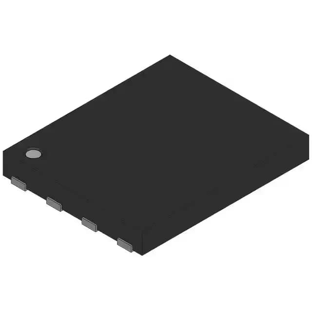
Renesas Electronics RJK03M2DPA-00#J5A

RJK03M2DPA-00#J5A N-Channel MOSFET, 30 V, 45 A, 2.8 mOhm

MPNRJK03M2DPA-00#J5A
End of Life

Renesas RJK03M2DPA-00#J5A, N-Channel MOSFET, 30 Vdss, 45 A continuous drain, 2.8 mOhm Rds(on) at 22.5 A, 10 V gate drive, 8-WPAK surface-mount package, 150 °C junction temperature.

$0.81538Ref. price · indicative, final on quote
Packaging8-WFDFN Exposed Pad
StockContact for availability
MOQ1 pcs
  • 100% new & originalTraceable channels only — no refurbs, no pulls, no remarked parts.
  • Date & lot codes on quoteStated per line before you commit; label photos on request.
  • MSL-compliant ESD packingMoisture-sealed bags with indicator cards; reels photo-verified.
  • PayPal buyer protectionPay by T/T, PayPal or Payoneer — card payments covered end to end.

Specifications

RJK03M2DPA-00#J5A Technical Specifications
ParameterValue
FET typeN-Channel
Mounting typeSurface Mount
Drain to source voltage30 V
Drive voltage (Max rds on, min rds on)4.5V, 10V
Current - continuous drain (Id) @ 25°C45A (Ta)
Power dissipation40W (Tc)
Operating temperature150°C (TJ)
PackageTape & Reel (TR)
Vgs±20V
TechnologyMOSFET (Metal Oxide)
Case8-WFDFN Exposed Pad
Rds on (Max) @ id, vgs2.8mOhm @ 22.5A, 10V
Gate charge (Qg) (Max) @ vgs21.2 nC @ 4.5 V
Input capacitance (Ciss) (Max) @ vds3850 pF @ 10 V

Product details

30 V, 45 A N-channel in an 8-WPAK — the switching FET for 12 V rails

The 8-WFDFN exposed-pad package (supplier device package 8-WPAK) is a small footprint for point-of-load converters, load switches, and battery protection circuits.

Gate charge and drive voltage — logic-level compatible

The FET fully enhances with a 4.5 V gate drive, making it compatible with 5 V logic or a 3.3 V-driven gate driver. Maximum gate charge is 21.2 nC at 4.5 V, so a modest gate-drive IC can switch it at several hundred kilohertz without excessive drive losses. Input capacitance is 3850 pF at 10 V drain-source — the gate-drive loop inductance and resistance need to be kept low to avoid ringing on the gate waveform.

Thermal budget and the exposed pad

Maximum power dissipation is 40 W at the case, but the 8-WFDFN package relies on the PCB copper area under the exposed pad to pull heat out.

Frequently asked questions

What is the closest functional second-source for RJK03M2DPA-00#J5A?

The NP179N055TUK--AY is a higher-voltage (55 V) and higher-current (180 A) N-channel MOSFET in a different package (Tray). It is not a pin-compatible drop-in — the 8-WPAK footprint differs — but it serves as a functional alternative for designs that need more voltage and current headroom. Gate charge is 240 nC at 10 V, which requires a stronger gate driver.