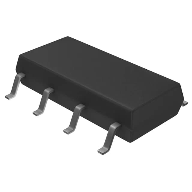
Renesas Electronics RJK0355DSP-00#J0

RJK0355DSP-00#J0 N-Channel MOSFET, 30V 12A 8-SOP

MPNRJK0355DSP-00#J0
End of Life

Renesas RJK0355DSP-00#J0 N-Channel MOSFET, 30 V Vdss, 12 A Id, 11.1 mOhm Rds(on) at 6 A / 10 V, 6 nC gate charge, 8-SOP surface-mount package, active production, ROHS3 compliant.

$1.28Ref. price · indicative, final on quote
Packaging8-SOIC (0.154", 3.90mm Width)
StockContact for availability
MOQ1 pcs
  • 100% new & originalTraceable channels only — no refurbs, no pulls, no remarked parts.
  • Date & lot codes on quoteStated per line before you commit; label photos on request.
  • MSL-compliant ESD packingMoisture-sealed bags with indicator cards; reels photo-verified.
  • PayPal buyer protectionPay by T/T, PayPal or Payoneer — card payments covered end to end.

Specifications

RJK0355DSP-00#J0 Technical Specifications
ParameterValue
FET typeN-Channel
Mounting typeSurface Mount
Drain to source voltage30 V
Drive voltage (Max rds on, min rds on)4.5V, 10V
Current - continuous drain (Id) @ 25°C12A (Ta)
Power dissipation1.8W (Ta)
Operating temperature150°C (TJ)
PackageTape & Reel (TR); Cut Tape (CT)
Vgs±20V
TechnologyMOSFET (Metal Oxide)
Case8-SOIC (0.154\", 3.90mm Width)
Rds on (Max) @ id, vgs11.1mOhm @ 6A, 10V
Gate charge (Qg) (Max) @ vgs6 nC @ 4.5 V
Input capacitance (Ciss) (Max) @ vds860 pF @ 10 V

Product details

30 V N-channel switch in a standard SOIC-8 footprint

The Renesas RJK0355DSP-00#J0 is a 30 V, 12 A N-channel power MOSFET in an 8-SOP package, built on a standard metal-oxide semiconductor process. It is designed for low-voltage load switching, DC-DC converter synchronous rectification, and power-rail OR-ing in 12 V and 24 V systems where board space is tight.

11.1 mOhm on-resistance — conduction loss at the load

That is the worst-case conduction loss figure for thermal budgeting: at 6 A the dissipation is 0.4 W, well within the 1.8 W package limit. The drive voltage range spans 4.5 V to 10 V, so a 5 V logic-level gate signal turns the channel on with higher resistance — expect roughly 1.4× to 1.6× the 10 V Rds(on) at 4.5 V.

6 nC gate charge — light driver load

Total gate charge is 6 nC at a 4.5 V gate drive. The 860 pF input capacitance at 10 V drain-source confirms the gate is easy to drive.

Thermal ceiling — 1.8 W in an SOP-8

Maximum power dissipation is 1.8 W at ambient temperature. The 12 A continuous drain rating is achievable only with the copper area on the PCB acting as a heatsink.

The part is ROHS3 compliant, meeting the current EU exemption rules for restricted substances.

Frequently asked questions

What is the maximum continuous drain current for RJK0355DSP-00#J0?

Continuous drain current is rated at 12 A at 25 °C ambient, but the 1.8 W power dissipation limit of the SOP-8 package means the practical current depends on the PCB copper area and airflow.

Can RJK0355DSP-00#J0 be used for 5V gate drive?

Yes. The drive voltage range includes 4.5 V, so a 5 V logic-level signal will turn the channel on. On-resistance at 4.5 V is higher than at 10 V — expect roughly 1.4× to 1.6× the 11.1 mOhm figure — so factor the higher conduction loss into the thermal budget.

What package does RJK0355DSP-00#J0 use?

It is surface-mount and fits the standard SOIC-8 land pattern.

Is RJK0355DSP-00#J0 RoHS compliant?

Yes, it is ROHS3 compliant, meaning it meets the current EU RoHS exemption rules including restrictions on the four phthalates.