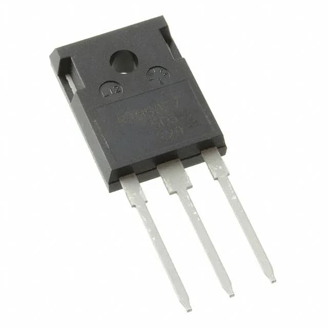
Renesas Electronics RJH65T46DPQ-A0#T0

RJH65T46DPQ-A0#T0 650V 80A Trench IGBT, TO-247A, Active

MPNRJH65T46DPQ-A0#T0
End of Life

Renesas RJH65T46DPQ-A0#T0 Trench IGBT, 650 V Vces, 80 A Ic, Vce(on) 2.4 V @ 15 V / 40 A, 138 nC gate charge, TO-247-3 / TO-247A package, through-hole, 175 °C Tj max, active lifecycle.

$5.48Ref. price · indicative, final on quote
PackagingTO-247-3
StockContact for availability
MOQ1 pcs
  • 100% new & originalTraceable channels only — no refurbs, no pulls, no remarked parts.
  • Date & lot codes on quoteStated per line before you commit; label photos on request.
  • MSL-compliant ESD packingMoisture-sealed bags with indicator cards; reels photo-verified.
  • PayPal buyer protectionPay by T/T, PayPal or Payoneer — card payments covered end to end.

Specifications

RJH65T46DPQ-A0#T0 Technical Specifications
ParameterValue
IGBT typeTrench
Input typeStandard
Mounting typeThrough Hole
Voltage - collector emitter breakdown650 V
Current - collector (Ic)80 A
Power - max340.9 W
Operating temperature175°C (TJ)
PackageTube
Gate charge138 nC
CaseTO-247-3
Test condition400V, 40A, 10Ohm, 15V
Switching energy450µJ (on), 550µJ (off)
Td (on/off) @ 25°C45ns/170ns
Vce(on) (Max) @ vge, ic2.4V @ 15V, 40A
Reverse recovery time100 ns

Product details

650 V / 80 A – the hard ceiling for the switching cell

The RJH65T46DPQ-A0#T0 is a Renesas Trench IGBT rated at 650 V collector-emitter breakdown voltage and 80 A continuous collector current.

Vce(on) and gate charge – the loss budget inputs

At 15 V gate drive and 40 A collector current, the typical Vce(on) is 2.4 V. The total gate charge is 138 nC.

Switching energy and timing – dead-time and heatsink planning

Tested at 400 V, 40 A, with a 10 Ω gate resistor and 15 V gate drive, the turn-on switching energy is 450 µJ and turn-off is 550 µJ. These per-pulse losses, multiplied by the switching frequency, give the total switching loss that the heatsink must dissipate. The turn-on delay (45 ns) and turn-off delay (170 ns) at 25 °C are inputs for dead-time calculation in a half-bridge – a 200 ns dead-time budget is typical to avoid shoot-through with these delay spreads.

Package and thermal path – TO-247A

Housed in a TO-247-3 through-hole package, with the supplier device package listed as TO-247A. The maximum junction temperature is 175 °C, and the maximum power dissipation is 340.9 W.

Lifecycle and sourcing posture

It is ROHS3 compliant.

Frequently asked questions

What is the maximum collector current and voltage rating of RJH65T46DPQ-A0#T0?

The maximum collector-emitter breakdown voltage is 650 V, and the maximum continuous collector current is 80 A. These are the absolute ratings that define the switching cell's voltage and current ceiling.

What is the Vce(on) and gate charge of RJH65T46DPQ-A0#T0?

The typical Vce(on) is 2.4 V at 15 V gate drive and 40 A collector current. The total gate charge is 138 nC, which determines the gate-driver average current requirement for a given switching frequency.