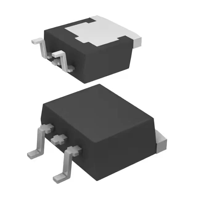
600 V, 35 A trench IGBT in a surface-mount LDPAK
The Renesas RJH60D3DPE-00#J3 is a trench-gate IGBT rated for a 600 V collector-emitter breakdown and 35 A continuous collector current. It is packaged in a surface-mount LDPAK (SC-83) suitable for automated pick-and-place assembly on power-stage PCBs. Trench IGBTs typically offer lower saturation voltage and faster switching than planar types, which matters in hard-switched topologies where conduction and switching losses both contribute to the thermal budget.
Conduction and switching loss — the thermal design numbers
Vce(on) is specified at 2.2 V maximum at Vge = 15 V and Ic = 17 A. That 2.2 V times the collector current gives the conduction loss per device, which must be sunk through the LDPAK package's thermal pad to the board copper. Total gate charge is 37 nC. At a 20 kHz switching frequency, the gate driver must supply 37 nC × 20 kHz = 0.74 mA average drive current; the peak current requirement depends on the desired turn-on/off time and the driver's source/sink capability. Switching energy is 200 µJ (turn-on) and 210 µJ (turn-off) tested at 300 V, 17 A, 5 Ω gate resistor, and 15 V gate drive. These values let the designer estimate total switching loss at the intended frequency and DC-link voltage.
Package and thermal path
The LDPAK (SC-83) is a surface-mount power package with an exposed metal tab on the top or bottom that serves as the collector connection and primary thermal path. The board layout must provide a copper area under the tab sized for the 113 W maximum power dissipation. Maximum junction temperature is 150 °C. The thermal design should keep TJ below this limit under worst-case load and ambient conditions, derating the 35 A collector current as needed.